Inspiriation
Hi Patrick
Fantastic work, cant wait to see more. Just what I needed to get me inspired to finish my F5X amp.
Looking forward to updates
Hi Patrick
Fantastic work, cant wait to see more. Just what I needed to get me inspired to finish my F5X amp.
Looking forward to updates
Hey Patrick, glad to see you back.
I was curious, what are the rough dimensions of the preamp boards?
I was curious, what are the rough dimensions of the preamp boards?
A friend is using F5XP & F5X for active crossover for his 2-way bookshelf.
He is going to use the F5XP to drive a purely passive filter network (LF & HF parallel).
These networks are followed by JFET follower, which then drives the F5XP.
I consider this a good solution indeed.
Patrick
I have choosen the same route some years ago and I still am convinced that this would be the right way to go. Currently I am building my F5X twins to have dedicated amps for each of the speaker transducers. But I am not sure yet how to solve the pre-amp problem: How to generate bandwith filtered balanced output signals as an input for my four power amplifiers from balanced and unbalanced input sources?
Using a F5X type of preamplifier SE driven could be considered to generated a balanced output as Patrick suggested.
Negative phase shorted to Gnd and gain compensated in the attenuator.
No additional internal converter (and hence added distortion), if that was the question.
Patrick
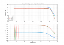
So I did an input output transfer matrix measurement with my F5X proto to find out how well this works.
The attached plot shows the measured voltage transfer matrix from both input terminals to both output terminals. A 11Ohms resistor across the output terminals served as load for measurement purpose. From each of the inputs the transfer to both outputs was measured while the other input was shorted to GND.
As one could see the bassband gain is pretty flat before it is turing into a (approx.) 2nd order roll-off at a corner frequency of about 2Mhz. Very impressive, but nothing new to most of the DIYers around here I guess. The phase also does not reveal any surprises. ( The phase wrapping spikes of the off diagonals H12 and H21 are due to measurement noise)
What could be read from the data is that the gain of the off-diagnoal elements is about 7.5dB whereas the gain of the diagonal elements is about 11dB. This means this amp driven single ended results in a difference of 3.5dB ( factor 1.5) in the amplitudes of both output terminals. Well, one could say this is still balanced, but not perfectly.
Since the topoloy of the F5X P is almost identical I anticipate a very similar result. I will keep on looking around for other options for SE - balanced transition. Conceptionally transformer would be ideal but I am not sure how far the parastics of the realizations will hurt.
Markus
Attachments
Any fully balanced amplifier with negative global feedback will have unequal amplitudes on the two phases when driven with a single ended signal.
I remember Nelson mentioned this also years ago.
The SE inputs are there for convenience, not for serious use.
Anyone who is serious about making optimal use of the F5X (or F5X Pre) should use differential over the entire chain.
To convert single ended to balanced properly, one could use a simple inverter circuit to generate the negative phase.
The simplest of that is of course an inverting opamp with unity gain.
The other option is a Blowtorch type circuit with grounded inverting input and unity gain.
Or as you said, transformer (fully passive and hence simplest).
Patrick
Last edited:
Hi Patrick,
Well come back to the F5X Pre!
I was sure that soon or later I can give the "Perfect Pre-amplifier" to the F5X 🙂
Best Regards,
Enrico
Well come back to the F5X Pre!
I was sure that soon or later I can give the "Perfect Pre-amplifier" to the F5X 🙂
Best Regards,
Enrico
Any fully balanced amplifier with negative global feedback will have unequal amplitudes on the two phases when driven with a single ended signal.
I remember Nelson mentioned this also years ago.
The SE inputs are there for convenience, not for serious use.
Anyone who is serious about making optimal use of the F5X (or F5X Pre) should use differential over the entire chain.
Patrick
Well, propably the SE - to balanced conversion is doing better then it looks on the first glance. Please find some related calcs attached
But well, I am not ready yet to skip the alternatives like transformers.
Markus
Attachments
Firstly your maths did not highlight the fact that you will not get perfect even harmonic distortion at the preamp stage already.
That is even assuming that the F5X Pre is perfectly symmetrical left & right.
Adding a F5X power amp does not cure that.
Secondly IMHO your problem is somewhat "self induced".
Your DAC (WM8740) already has fully differential outputs.
You only need to tap them out and add a level shifter (or simply a coupling cap).
And if you are really fuzzy, a source follower per phase as buffer.
Why make all these other compromises ?
Patrick
Hi Patrick,
just to refresh my memory I reread the pdf´s you posted at the beginning of this thread and had a look at the shunt attenuator again.
I did some calculations a while ago to try and make one for my X-BOSOZ (to replace a 24 step switch) but did not succeed with a limited amount of relays to get even steps.
I´ve calculated the first 15 steps or so (10k series resistors), later steps will get smaller and smaller if you use all (2^8) 256 steps and end at -48dB for all relays paralleled.
resistance dB
20000 -6,0
10000 -9,5
6667 -12,0
5000 -14,0
4000 -15,6
3333 -16,9
2857 -18,1
2500 -19,1
2222 -20,0
2000 -20,8
1818 -21,6
1667 -22,3
1538 -22,9
1429 -23,5
1333 -24,1
So the first steps are quite big (-6dB, -3,5dB, -2,5dB) and get smaller after that. When going for more total attenuation (-75dB) this will be even more pronounced.
Am I overlooking something?
William
William,
Yes that is correct.
Bear in mind the F5X Power Amp will take 2Vrms per phase at the input before clipping.
And most of the sources today has output levels of also around 2V rms.
So in theory one can use a unity gain buffer in between, or nothing.
Since the F5X Pre has a gain of ~10, I expect the most used range of the attenuator to be between -20dB & -40dB.
My current setup (not F5 based) is actually pretty much the same, so I know what to expect.
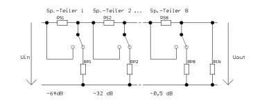
But you are welcome to use one of those constant impedance attenuators if this is what you all agreed upon (see attached).
We'll make a special "public" version then with max. 8 relays per channel.
The problem with such a solution is that the signal goes through a chain of resistors and relay contacts in series.
We compared those to just a potential divider with 2 resistors. Huge difference.
So we ourselves will stick to our own solution.
The balanced input signal will only see 2 fixed series resistors and a shunt resistor.
The latter being made up of a varying number of resistors and relay contacts, BUT in parallel.
Patrick
Yes that is correct.
Bear in mind the F5X Power Amp will take 2Vrms per phase at the input before clipping.
And most of the sources today has output levels of also around 2V rms.
So in theory one can use a unity gain buffer in between, or nothing.
Since the F5X Pre has a gain of ~10, I expect the most used range of the attenuator to be between -20dB & -40dB.
My current setup (not F5 based) is actually pretty much the same, so I know what to expect.
But you are welcome to use one of those constant impedance attenuators if this is what you all agreed upon (see attached).
We'll make a special "public" version then with max. 8 relays per channel.
The problem with such a solution is that the signal goes through a chain of resistors and relay contacts in series.
We compared those to just a potential divider with 2 resistors. Huge difference.
So we ourselves will stick to our own solution.
The balanced input signal will only see 2 fixed series resistors and a shunt resistor.
The latter being made up of a varying number of resistors and relay contacts, BUT in parallel.
Patrick
Attachments
Hi Patrick,
that´s what I thought. I´ve used a balanced attenuator for many years with an Elma 24 position switch (at the output of my X-BOSOZ) until the noises from the switch became too much for me. I´ve used it for the reasons you mention above.
I then tried to make one with just an 8 bit AD converter and 8 relays but that was not possible (as it is with the constant impedance one where you can have defined dB steps). I now have a constant impedance one but since then discovered Arduino so I could try a shunt version with relays which also has the advantage of much lower output impedance with the X-BOSOZ.
At the moment I´m normally in the -50 to -35dB region (X-BOSOZ x4, Aleph-X x10 and Bastani Mandelas with almost 100dB). If I have to turn the volume down for background music it is more like -65dB.
So I would go for the shunt version but maybe with some different values to get the range a bit further down.
William
That is easy.
You just increase the series resistor from say 10k to 22k, then you get 6dB extra.
Or to 100k for 20dB.
Alternatively, stay with 10k for series, and lower everything else shunt by factor of 8, or 10.
Then no need to change circuit, just resistor values.
Patrick
You just increase the series resistor from say 10k to 22k, then you get 6dB extra.
Or to 100k for 20dB.
Alternatively, stay with 10k for series, and lower everything else shunt by factor of 8, or 10.
Then no need to change circuit, just resistor values.
Patrick
Hi Patrick,
I will try to make a spreadsheet for this where one can set series resistors and the 8 other ones to play with. I suppose you won´t use the full 8bit resolution (256 positions) for a lookup table?
William
I will try to make a spreadsheet for this where one can set series resistors and the 8 other ones to play with. I suppose you won´t use the full 8bit resolution (256 positions) for a lookup table?
William
We use the full 8 bits, but in 1dB steps or nearest, except for the few initial steps as you pointed out.
So you don't need to press 256 times to go from top to bottom.
Patrick
So you don't need to press 256 times to go from top to bottom.
Patrick
We discussed this topic once in private while we were doing the F5X PCBs.
I just happened to be doing some literature search today, so I thought I would post it again.
It is still relevant, epecially as we use SMT components increasingly.
There are many DIY board being offered with gold plating as a selling point.
As a rule, we never get any PCBs made with gold platings, only with tin solder (HASL).
There was once when the supplier made a mistake and supplied flash gold.
We ended up stripping all the gold with a double tinning process.
The reason ?
Not because we want to save a few dollars, but because of gold embrittlement of solder joints.
In fact, this not only applies to PCBs but alo to all connectors with soldered joints.
We also strip off gold from connectors by tinning and then removing with solder wick, twice.
Here are a few links for thoe interested to know more.
http://www.eptac.com/webinars/presentations/eptac_10_17_12.pdf
Microscopy and Microanalysis - Fulltext - Microscopy of Solder Joint Failures Due to Gold Intermetallic Embrittlement - Cambridge Journals Online
http://www.dfrsolutions.com/wp-content/uploads/2013/12/Gold-Embrittlement-in-Leadfree-Solder.pdf
http://www.semlab.com/papers/goldembrittlementofsolderjoints.pdf
http://www.diyaudio.com/forums/construction-tips/260017-solder-gold-copper.html#post4015182
http://www.diyaudio.com/forums/loun...ch-preamplifier-part-ii-1059.html#post3935630
As far as we know, there is no real threshold in plating thickness where gold embrittlement cannot be a concern.
It also appears that it is particularly an issue for SMT components.
The only application where we would specify gold plating on PCBs are edge connectors.
But there we would specifiy electro-plated hard gold, rather than the usual ENIG.
http://dcchapters.ipc.org/assets/pnw/presentations/20030925_finishes.pdf
Patrick
Patrick,
Thanks for sharing all this information.
I didn't know that the ENIG finishing that is the most common from the PCB manufacturers can perform so bad results with the SMD reflow.
Regards,
Enrico
Thanks for sharing all this information.
I didn't know that the ENIG finishing that is the most common from the PCB manufacturers can perform so bad results with the SMD reflow.
Regards,
Enrico
Today's consumer products are not designed to last more than a few years.
Else the entire electronic industry will collapse.
Patrick
Else the entire electronic industry will collapse.
Patrick
- Home
- Amplifiers
- Pass Labs
- The F5X Preamp