Hello everyone I ask you who have more knowledge than me to help me solve an enigma.
Is the emitter follower really 100% negative feedback?
I bring you some writings of an ex audio designer translated, where he questions the negative feedback of an emitter follower, I would really like to understand where the truth lies.
"The RADIOTRON DESIGNER'S HANDBOOK (by the famous RCA - radio corporation of america - FOURTH EDITION by LANGFORD and SMITH - 1952 - the foundation of electronics and also of a lot of hi-fi of our times, 1482 pages) at page 317, chap. 7.2 titled the following sentence talking about the "cathode follower" of a triode:
"As a result of 100% negative voltage feedback inherent in cathode follower, both the distortion and the output impedance may be very low".
I personally add that the same sentence could be applied also to a transistor in EMITTER FOLLOWER.
But is this REALLY true? This is written and handed down, all right, but to me personally a long time ago, a spontaneous question arose:
QUESTION: If the transistor does NOT amplify in voltage (but only in current,) does it mean that it's 100% negative feedback in VOLTAGE?
Nice question
Emitter follower properties:
1 - high input resistance
2 - low output resistance
3 - high current gain
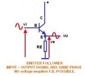
4 - POSITIVE voltage gain, but less than unity
We should think about the fact that a transistor is a CURRENT AMPLIFIER (by nature of the device), and not a VOLTAGE AMPLIFIER, so, if it amplifies in CURRENT (as of its nature, in the simplest circuit that exists), can it be blamed not to amplify also in voltage? but this could be taken as pure philosophy ....
Maybe this could be valid for a tube or mosfet that are voltage-driven devices (but even there it may not be true), then I have drawn the equivalent circuit of the transistor in emitter follower and I have noticed that NEGATIVE FEEDBACK DOES NOT EXIST, neither in current nor in voltage and we will see later why.
Current Negative Feedback
The condition for NEGATIVE FEEDBACK is:
- The decrease of the maximum amplification obtainable from the circuit itself (that is less than that which can be obtained in the use of the same device without the application of nf)
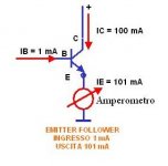
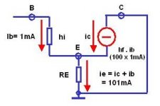
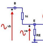
If the OUTPUT is on the EMITTER leg, (and with no load on the collector), by definition the transistor amplifies ONLY IN CURRENT (MAXIMUM CURRENT as we will see) and the resistor RE is used ONLY to LIMIT the amount of the OUTPUT current, otherwise the transistor may burst.
Not putting the RE, the transistor ALWAYS AMPLIFIES ONLY IN CURRENT and its AMPLIFICATION is of the same ENTITY as WHEN the RESISTANCE is there. So emitter resistance is not able to change things. The amplification factor of the stage, DOES NOT CHANGE AT ALL.
The current amplification factor of a transistor is called BETA (also called hfe) which has a precise value like 11, 26, 54, 77, or 126 or 12000.
This parameter says that if at the input of the transistor I put 1mAh of current (direct or alternating), in the case of an EMITTER FOLLOWER, at the output I can get back a quantity of current BETA times bigger.
Where does the transistor get it from? From the power supply.
If the transistor amplifies 100 (i.e. its BETA or hfe is = 100), sucking current from the DC supply, at least, we can have on the collector circuit a current 100 times bigger, i.e.: 100mAh.
But the output of this current, in this case, is taken from the emitter circuit, and there the BASE current (the input one) ends up too, so what we will get in the example is a nice 101 mAh output. MAXIMUM AMPLIFICATION in CURRENT. Actually already a bit more, we have also recovered the base current supplied by the external signal.
We have these 101 milliampere even if we remove the RE, and they can be measured with an ammeter (see FIG.1). Now the first result is to see that on the EMITTER Node, the two currents add up and do not subtract. If they subtracted there would already be something to think about, maybe a negative feedback: that is something tends to remove instead of adding. This can also be verified in the equivalent circuit for alternating signals, shown below (in FIG. 3 and 4).
So we can state that the RE CANNOT control the output current on the emitter leg. This means local current negative feedback = ZERO, up to the limit of its operation (saturation or burnout of the device or LIMITATION due to the series resistance at the input).
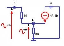
Voltage Negative Feedback
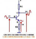
Remember that due to the MILLER effect, the resistance seen from the input is NOT anymore only the base resistance (hie) plus the emitter one (ex: if RE= 470 ohm, that is 1000+ 470=1470 ohm), but instead to "hie" (1000 ohm) is added a resistance of 470 ohm (RE), multiplied by the BETA (100). The TOTAL input resistance of the transistor ONLY will be = 1000 + 470 x 100 = 48.000 ohm. In the game, is lost in practice, part of the voltage signal that arrives at the input (BASE), in the case of the example about one 48th.
If we have lost part of the input signal, can we think of the effect of a voltage feedback? And if so, how much is it worth?
If the value of the input voltage is 1 volt and 0,98 volt come out of the emitter (we have lost let's say one 50th, or about 2% - the base current in this case would be 1 Volt/48.000 ohm), the amount of the negative feedback, if this is the case, how much is it? we will see in a moment.
(Moreover I am wondering: the same thing is done by a "miserable" POTENTIOMETER (lose voltage on the way) on two resistors in partition, isn't it...?)
Anyway If we lost half of the signal (0.5 volts) we would have lost 6 dB (and we could talk about 6 dB of feedback), if we lose only 0.3 volts, we have a loss of about 3 dB, if we lose 2% of VOLT the attenuation would be 0.175 dB.
If it were really negative feedback we would be at almost unlistenable levels, since around ZERO db of feedback is SYNONYM OF TOTAL ABSENCE OF negative voltage feedback.
A little consideration also about linearity and output impedance of the BJT follower.
The output resistance is not equal to RE, but for a transistor it is normally lower even without the use of feedback and much lower than for voltage-driven devices (FET and TRIODES). This also means LESS influence due to the external load that is in parallel with RE.
The linearity of a BJT follower is normally very high, because the linear zone and the active zone are practically coincident, which is not the case for voltage-driven devices that have respectively the active zone after a few volts (FET) or tens of volts (TRIODES)."
Every thought is appreciated, thank you.
Is the emitter follower really 100% negative feedback?
I bring you some writings of an ex audio designer translated, where he questions the negative feedback of an emitter follower, I would really like to understand where the truth lies.
"The RADIOTRON DESIGNER'S HANDBOOK (by the famous RCA - radio corporation of america - FOURTH EDITION by LANGFORD and SMITH - 1952 - the foundation of electronics and also of a lot of hi-fi of our times, 1482 pages) at page 317, chap. 7.2 titled the following sentence talking about the "cathode follower" of a triode:
"As a result of 100% negative voltage feedback inherent in cathode follower, both the distortion and the output impedance may be very low".
I personally add that the same sentence could be applied also to a transistor in EMITTER FOLLOWER.
But is this REALLY true? This is written and handed down, all right, but to me personally a long time ago, a spontaneous question arose:
QUESTION: If the transistor does NOT amplify in voltage (but only in current,) does it mean that it's 100% negative feedback in VOLTAGE?
Nice question
Emitter follower properties:
1 - high input resistance
2 - low output resistance
3 - high current gain
4 - POSITIVE voltage gain, but less than unity
We should think about the fact that a transistor is a CURRENT AMPLIFIER (by nature of the device), and not a VOLTAGE AMPLIFIER, so, if it amplifies in CURRENT (as of its nature, in the simplest circuit that exists), can it be blamed not to amplify also in voltage? but this could be taken as pure philosophy ....
Maybe this could be valid for a tube or mosfet that are voltage-driven devices (but even there it may not be true), then I have drawn the equivalent circuit of the transistor in emitter follower and I have noticed that NEGATIVE FEEDBACK DOES NOT EXIST, neither in current nor in voltage and we will see later why.
Current Negative Feedback
The condition for NEGATIVE FEEDBACK is:
- The decrease of the maximum amplification obtainable from the circuit itself (that is less than that which can be obtained in the use of the same device without the application of nf)
If the OUTPUT is on the EMITTER leg, (and with no load on the collector), by definition the transistor amplifies ONLY IN CURRENT (MAXIMUM CURRENT as we will see) and the resistor RE is used ONLY to LIMIT the amount of the OUTPUT current, otherwise the transistor may burst.
Not putting the RE, the transistor ALWAYS AMPLIFIES ONLY IN CURRENT and its AMPLIFICATION is of the same ENTITY as WHEN the RESISTANCE is there. So emitter resistance is not able to change things. The amplification factor of the stage, DOES NOT CHANGE AT ALL.
The current amplification factor of a transistor is called BETA (also called hfe) which has a precise value like 11, 26, 54, 77, or 126 or 12000.
This parameter says that if at the input of the transistor I put 1mAh of current (direct or alternating), in the case of an EMITTER FOLLOWER, at the output I can get back a quantity of current BETA times bigger.
Where does the transistor get it from? From the power supply.
If the transistor amplifies 100 (i.e. its BETA or hfe is = 100), sucking current from the DC supply, at least, we can have on the collector circuit a current 100 times bigger, i.e.: 100mAh.
But the output of this current, in this case, is taken from the emitter circuit, and there the BASE current (the input one) ends up too, so what we will get in the example is a nice 101 mAh output. MAXIMUM AMPLIFICATION in CURRENT. Actually already a bit more, we have also recovered the base current supplied by the external signal.
We have these 101 milliampere even if we remove the RE, and they can be measured with an ammeter (see FIG.1). Now the first result is to see that on the EMITTER Node, the two currents add up and do not subtract. If they subtracted there would already be something to think about, maybe a negative feedback: that is something tends to remove instead of adding. This can also be verified in the equivalent circuit for alternating signals, shown below (in FIG. 3 and 4).
So we can state that the RE CANNOT control the output current on the emitter leg. This means local current negative feedback = ZERO, up to the limit of its operation (saturation or burnout of the device or LIMITATION due to the series resistance at the input).
Voltage Negative Feedback
Remember that due to the MILLER effect, the resistance seen from the input is NOT anymore only the base resistance (hie) plus the emitter one (ex: if RE= 470 ohm, that is 1000+ 470=1470 ohm), but instead to "hie" (1000 ohm) is added a resistance of 470 ohm (RE), multiplied by the BETA (100). The TOTAL input resistance of the transistor ONLY will be = 1000 + 470 x 100 = 48.000 ohm. In the game, is lost in practice, part of the voltage signal that arrives at the input (BASE), in the case of the example about one 48th.
If we have lost part of the input signal, can we think of the effect of a voltage feedback? And if so, how much is it worth?
If the value of the input voltage is 1 volt and 0,98 volt come out of the emitter (we have lost let's say one 50th, or about 2% - the base current in this case would be 1 Volt/48.000 ohm), the amount of the negative feedback, if this is the case, how much is it? we will see in a moment.
(Moreover I am wondering: the same thing is done by a "miserable" POTENTIOMETER (lose voltage on the way) on two resistors in partition, isn't it...?)
Anyway If we lost half of the signal (0.5 volts) we would have lost 6 dB (and we could talk about 6 dB of feedback), if we lose only 0.3 volts, we have a loss of about 3 dB, if we lose 2% of VOLT the attenuation would be 0.175 dB.
If it were really negative feedback we would be at almost unlistenable levels, since around ZERO db of feedback is SYNONYM OF TOTAL ABSENCE OF negative voltage feedback.
A little consideration also about linearity and output impedance of the BJT follower.
The output resistance is not equal to RE, but for a transistor it is normally lower even without the use of feedback and much lower than for voltage-driven devices (FET and TRIODES). This also means LESS influence due to the external load that is in parallel with RE.
The linearity of a BJT follower is normally very high, because the linear zone and the active zone are practically coincident, which is not the case for voltage-driven devices that have respectively the active zone after a few volts (FET) or tens of volts (TRIODES)."
Every thought is appreciated, thank you.
Attachments

Last edited:
My thoughts? Hard to have any valuable ones as your arguments are difficult and incomplete. It is good to analyze such simple circuits for thorough understanding. Points for that. First step is to really understand the hfe model and the definitions of some of the terms you use like Re. Then apply it and let the math tell you the answer. As a side question, are you of the feedback is bad school?
RE = emitter resistance.My thoughts? Hard to have any valuable ones as your arguments are difficult and incomplete. It is good to analyze such simple circuits for thorough understanding. Points for that. First step is to really understand the hfe model and the definitions of some of the terms you use like Re. Then apply it and let the math tell you the answer. As a side question, are you of the feedback is bad school?
Anyway I'm not of the feedback good or bad school, I'm just trying to understand if the emitter follower is really negative feedback or not.
Last edited:
Another question to ponder. Does the relatively linear triode tube have negative feedback? How does it get so linear when in theory, current is proportional to the applied field to the three halves power?
The input signal to the transistor is between the base and emitter. The output signal (across the emitter resistor/load) is in series with the input signal. In such a direction that an increase in output tends to oppose the change applied to the input. Therefore the feedback is negative.RE = emitter resistance.
Anyway I'm not of the feedback good or bad school, I'm just trying to understand if the emitter follower is really negative feedback or not.

Oh, that’s a can of worms. Triodes have internal thermal feedback which causes them to be inherently relatively linear. Don’t tell anit-feedbackers that, though.Another question to ponder. Does the relatively linear triode tube have negative feedback? How does it get so linear when in theory, current is proportional to the applied field to the three halves power?
In an emitter follower the output is in series with the signal driving the output in such a way, as the input has to be greater than the output. This means, the output is opposing the input, which is negative feedback. The gain is slightly less than one because a little (AC) voltage is required to drive the base emitter junction. For a perfect unity gain, a BJT must have zero input impedance, which is not attainable as bases require energy to be driven.
This means, the output is opposing the input, which is negative feedback.
Sorry what do you mean exactly?The input signal to the transistor is between the base and emitter. The output signal (across the emitter resistor/load) is in series with the input signal. In such a direction that an increase in output tends to oppose the change applied to the input. Therefore the feedback is negative.
The output is not in phase opposition compared to the input as is common in negative feedback.
Last edited:
As you drive the base voltage more positive, the emitter voltage also goes more positive. That OPPOSES a change in the base-to-emitter voltage.
And what does this mean? That there is negative feedback in voltage or current?As you drive the base voltage more positive, the emitter voltage also goes more positive. That OPPOSES a change in the base-to-emitter voltage.
The defining condition for negative feedback is having a portion of the output subtracting from/opposing the input. Under this condition, an input has to be bigger compared to when it is not opposed. The opposite happens when an input is aided by a portion of the output. In this case, the input needed is smaller.
It does not matter if you represent the transistor as a current gain, a transconductance or a voltage gain. The feedback equation form remains the same. That being overall gain for the stage (G) equal to the forward gain (A) over one plus the forward gain times the feedback gain (B).
G=A/(1+AB)
For an emitter follower B=1 100% feedback. If using transconductance, A=gm*Rload
I encourage you to derive this from the node equations for the emitter follower.
G=A/(1+AB)
For an emitter follower B=1 100% feedback. If using transconductance, A=gm*Rload
I encourage you to derive this from the node equations for the emitter follower.
What do you mean?In this case, the input needed is smaller.
A is the β of the transistor?It does not matter if you represent the transistor as a current gain, a transconductance or a voltage gain. The feedback equation form remains the same. That being overall gain for the stage (G) equal to the forward gain (A) over one plus the forward gain times the feedback gain (B).
G=A/(1+AB)
For an emitter follower B=1 100% feedback. If using transconductance, A=gm*Rload
I encourage you to derive this from the node equations for the emitter follower.
Yes, if you use a current gain as the gain element in the setup of the for circuit equations.
And B why is 1?Yes, if you use a current gain as the gain element in the setup of the for circuit equations.
I haven't worked it out, but to be precise, I think A in the current gain analysis case is actually (1+beta). Details details!
B=1 because all of the output is fed back to the input without attenuation. B is for most applications <=1.
Keep in mind the input is the input from the transistors perspective. The difference in the base to emitter voltage.
Interesting what you write, but why shouldn't i separate the voltage gain from the current gain discussion? aren't they separate things? one take place in the collector leg and the other in the emitter leg.It does not matter if you represent the transistor as a current gain, a transconductance or a voltage gain. The feedback equation form remains the same.
- Home
- Amplifiers
- Solid State
- The Emitter Follower Enigma