Hi Zung,
I just spent the better part of a few hours reading that thread and learned a lot...but as you say, little mention of selecting the bypass cap, only a passing mention by peufeu:
--------------------------------------------------------------------------------------------------------------
peufeu
Member
Does the 100nF cap between the driver emitters help with the hFe mismatch?Answer: no, it is there only to help turn-off. No difference in the input current with and without the cap.
-------------------------------------------------------------------------------------------------------------------
And that post was analyzing a 100 nF cap between driver emitters, the cap I am talking about (and perhaps you as well) is between driver bases at the bias spreader, so Anatech perhaps misunderstood by telling you to go back and read the thread.
I think there is a kernel of good info in peufeu's reply namely; if the VAS drive to the driver is truly differential there should be little difference. However, in many (most?) amplifiers the VAS is single-ended with a current mirror, with the two split by the bias spreader. In this case the bias spreader is carrying all differential VAS current to the drivers on top of the quiescent bias current for the driver. And if it really makes no difference, why do so many amp designs include one or more caps as bias spreader bypass? If it is just to lower the HF impedance of the bias network compensating for a slow bias transistor, I can see that. In my case I am wondering if the failure of the bias spreader transistor was due to excessive current...I am sure my ignorance of this topology is obvious at this point.
I'll keep investigating as I find time, the day is half gone and I need to get work done. I'll report back if I find any new information.
Cheers!
Howie
I'm just curious: many commercial brands I like (Ayre, Electrocompaniet, Parasound, etc,) use a very small cap, 1uF or less, for bypassing the bias spreader. And the reverse is also true, but I can't name names for fear of ending up in Guantanamo. 🙂
I normally only mess with stuff that glow in the dark, and they're more straightforward: deal with the neg. bias supply with the same respect as the main supply, plus the bias must come up long before the high voltage, and that's it.
I normally only mess with stuff that glow in the dark, and they're more straightforward: deal with the neg. bias supply with the same respect as the main supply, plus the bias must come up long before the high voltage, and that's it.
The application of a large electrolytic as bias spreader bypass seems to have some correlation with the pre-driver or VAS output topology which makes sense. John Curl only uses a 200 pF in the fully differential JC1, Nelson Pass a 220 uF in the A-40 which has a single-ended VAS output, but 150 nF in the differentially driven Stasis 2. Likewise the Bryston 3B with bias drive similar to the Luxman M4000 with a single-ended drive through the spreader to a current source uses only a 100 nF...given the preponderance of existing design choices I think Luxman only using two 220 nF caps as a bypass is probably an intentional choice, but it is interesting to note the schematic and PCB were laid out for a 330 uF...go figure. Time to move on.
Cheers!
Howie
Cheers!
Howie
Bob Cordell's power amp textbook discusses the tradeoffs pretty thoroughly.

Hi Mark,
I read through Bob's book and only found the very short mention of using a "usual" cap as bypass. Can you help me find where in the book he discusses the bias bypassing?
Cheers,
Howie
I read through Bob's book and only found the very short mention of using a "usual" cap as bypass. Can you help me find where in the book he discusses the bias bypassing?
Cheers,
Howie
Thanks indra1,
Yes, the speedup capacitor is discussed extensively in that chapter, and exhaustively covered in the thread:
Cheers!
Howie
Yes, the speedup capacitor is discussed extensively in that chapter, and exhaustively covered in the thread:
Power amp OUTPUT STAGE measurements shootout
With apologizes to those who understand the application of bias spreaders for different OS topologies better than I, the purpose and effect when coupling the emitters of the output stage is slightly different than the capacitor presented across the bias spreader network at the bases of the driver. Nevertheless, the actual value of capacitance in this application seems less than critical, at least I have not found a discussion of how to calculate an exact value.Cheers!
Howie
Howie,
As you pretty well know the voltage across the bias spreader and the current through it as they are often fed from a current source, ohms law will give you the apparent resistance.
So a typical value might be 1.2 volts at 10 mA would yield via Ohm’s law 1.2/.01=120. So for conservative use a bypass capacitor would be set for a decade below the passband. 1/( 2 x pi x f x R) = C. Using 2 Hz as a decent low frequency cut off would best be served by a standard capacitor value of 1,000 uFd. However at low frequencies the bias setting circuit will still have plenty of gain and not be as dependent on the bypass capacitor. However as the frequency increases the transistor’s gain decreases. So instead of using a lowpass frequency value, it is often practical to use a bypass frequency where the current gain of the transistor involve has had the DC gain drop in half.
For a typical small signal transistor this can be few hundred megahertz. So just a small bypass capacitor will work. Often as small as 47 pF.
Now as the cost of adding such a small capacitor is trivial and the cost pretty much doesn’t increase as the value goes up, the capacitor value can be increased based on cost!
So you can select a decent size electrolytic capacitor based on the math and most likely not notice any change by listening or measurement.
But even with an electrolytic capacitor a small inexpensive bypass capacitor is useful. However a ceramic capacitor that changes capacitance with voltage can often have other issues that affect performance even though in this application they have a constant voltage. (As an example never use an X7R capacitor here!)
So if you look at practical circuits there is reason for confusion. A calculated circuit might have a bypass electrolytic capacitor, but a quick measurement in a properly constructed circuit should show it has no effect. Practical wiring and moving some parts to the heatsink probably will need some bypass capacitance.
Last edited:
Hi Ed!
Yes, I was thinking the two limiting functions were the drop in gain at HF and perhaps a HP corner at some low frequency but of course this is basically a DC amp, so forget about the LF corner...duh. Your analysis makes sense and the only measure any reference mentions is HF impedance, so a small cap is dictated. This seems to be reinforced by so many amps having just some hundreds of nF of film cap serve this function. I apologize to anyone put off by my stumbling around this small issue, but I am used to finding concise treatise on most issues on which I am interested, either in my books or on line...but not for this one...it must be too trivial for most skilled in amp design!
Thanks for the analysis Ed, and I hope all is well in PA...cold here tonight after a week of 70° F+! A disastrous early spring for our fruit plants...
Back to buttering TO-3 micas....yuck.
Cheers!
Howie
Howie,
When you supply me with the full circuit diagram including end stage bias setting, I could show you with a few LTSpice runs the effect on THD and IMD for different caps across the Bias Spreader.
Hans
When you supply me with the full circuit diagram including end stage bias setting, I could show you with a few LTSpice runs the effect on THD and IMD for different caps across the Bias Spreader.
Hans
Hi Hans!
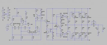
That is a very generous offer, here is the service manual and a slightly clearer schematic. I apologize in advance for the poor image quality, it is the best I have been able to find 🙁. I am very interested in knowing what you think about this design and spreader bypass cap selection, I have a feeling just as Bob Cordell hints at by calling the selection just a "usual" cap, it is not a huge issue one way or the other but it would be good to know. The circuit like most bias spreaders looks to me to just be a two-terminal DC regulator with a cap across it to lower it's AC impedance. The difference between it and the 'speedup' caps is the fact that it is not just between output emitters in order to drain charge off faster. I look forward to your findings, as will Zung and likely others here, given the paucity of information available elsewhere!
Cheers!
Howie
p.s. I have been replacing the 2SD424/2SB554 pairs with MJ21194/MJ21193 successfully in the last few years, and have in this amp as well due to unavailbility of REAL Toshiba 2SD/2SB parts...
Last edited:
Howard,
I have entered your amp's essentials in LTSpice with a 8R speaker load, but without the short circuit protection.
Also the power supply caps are missing, because in LTSpice power supply is rock solid and adding caps doesn´t improve anything.
The same for paralleling caps, it´s just the bigger one that matters because they are ideal caps as long as no serial inductance is specified.
The Cap in your situation is C8 that I will vary for several values.
However since the circuit diagram is hardly readable, I have left the task to you to tell me the resistor and capacitor values as specified in the manual.
This would take me too much time.
Once defined, I will run LTSpice for THD and IMD.
Hans
Attachments
Hello Hans,
I have updated the .asc file with the actual values from the PCBs other than the semiconductors, it is attached. I was unable to find the models for the output semis you loaded, so I had not tried a sim yet. The Spice models for the MJ21193 and MJ21194 output devices in this amp are here, for some reason I could not attach them, very odd.
Thank you so much once again, I look forward to some data!
Cheers,
Howie
Attachments
Hi Howard,
Here you are, two things had to be changed:
1) R4 into 610R to equalize the DC current through Q3 and Q4 and
2) C3 from 47pF into 1nF. This 47pF must definitely be an error.
But for the rest everything you did seemed to be O.K.
There is no difference whatsoever to find in all sims when varying C8 between 440nF and 440uF.
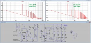
In the first attachment I have simmed THD with both 35mA and 70mA per output pair, so in total between 105mA and 210mA at 1Watt@8R output power.
It's obvious that with the transistors used, 70mA per output pair or 210mA in total is the better one, but in your case it may differ.
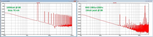
The second sim shows at the left side THD at 100watt@8R and IMD 19Khz+20Khz at 1Watt peak at the right side.
So, the answer to your question relating the Cap on the bias spreader, being independent from the used transistors, has been given with the simulations. 440nF is adequate and anything larger is not adding any benefit.
It's a bit unusual circuit diagram with lots of caps, but it still performs perfectly with relatively low distortion.
Hans
Here you are, two things had to be changed:
1) R4 into 610R to equalize the DC current through Q3 and Q4 and
2) C3 from 47pF into 1nF. This 47pF must definitely be an error.
But for the rest everything you did seemed to be O.K.
There is no difference whatsoever to find in all sims when varying C8 between 440nF and 440uF.
In the first attachment I have simmed THD with both 35mA and 70mA per output pair, so in total between 105mA and 210mA at 1Watt@8R output power.
It's obvious that with the transistors used, 70mA per output pair or 210mA in total is the better one, but in your case it may differ.
The second sim shows at the left side THD at 100watt@8R and IMD 19Khz+20Khz at 1Watt peak at the right side.
So, the answer to your question relating the Cap on the bias spreader, being independent from the used transistors, has been given with the simulations. 440nF is adequate and anything larger is not adding any benefit.
It's a bit unusual circuit diagram with lots of caps, but it still performs perfectly with relatively low distortion.
Hans
Attachments
An often mentioned "scary monster" is clipping. When playing the 1812 Overture beyond the clipping point, does the bias spreader end-to-end voltage change? How badly does this affect the output stage bias { for believers in "the Barney Oliver criterion" } , increasing crossover distortion? How long does it take to recover to the correct end-to-end voltage? I.e. how long does it take to charge or discharge the capacitor in parallel with the bias spreader?
When clipping would happen without load, voltage on the Cap remains practically constant.
With load attached, long before the above clipping, the max current protection comes into action, also leading to a controlled clipping.
This will indeed discharge the bias spreader cap on the negative going slope, but this has to be a severe overload condition where discharging and recharging with the 440nF takes place between 50 to 100 usec.
When using a larger Cap, voltage fluctuations on the spreader will become smaller but it will also take longer to recover.
But I think this is what we call in the Netherlands "searching for snails on salty water".
When music played that loud that clipping occurs with this very amp, I would be more concerned for my eardrums.
Hans
Last edited:
Wow Hans,
I just looked at both of the driver boards themselves and both are stuffed with a 47 pF cap at C3, and the tail resistor at R4 is 390 ohms 1W, and R11 is 100 ohms, 1W, all parts agree with the schematic, so although it may have been a design error, it wasn't a stuffing error. Q3 & 4 are 2SC805A rated at 200 mA Hfe ~100, Ft 160 MHz and mounted on heatsinks. Q5 is a 2SA762 rated at 2 A, Hfe ~100@400 mA Ft 80 MHz, also on heatsinks. What problem did you see simmed with the 47 pF and 390 ohm in place?
Cheers!
Howie
Thank you yet again, for your time and effort!Hi Howard,
Here you are, two things had to be changed:
1) R4 into 610R to equalize the DC current through Q3 and Q4 and
2) C3 from 47pF into 1nF. This 47pF must definitely be an error.
But for the rest everything you did seemed to be O.K.
There is no difference whatsoever to find in all sims when varying C8 between 440nF and 440uF.
In the first attachment I have simmed THD with both 35mA and 70mA per output pair, so in total between 105mA and 210mA at 1Watt@8R output power.
It's obvious that with the transistors used, 70mA per output pair or 210mA in total is the better one, but in your case it may differ.
The second sim shows at the left side THD at 100watt@8R and IMD 19Khz+20Khz at 1Watt peak at the right side.
So, the answer to your question relating the Cap on the bias spreader, being independent from the used transistors, has been given with the simulations. 440nF is adequate and anything larger is not adding any benefit.
It's a bit unusual circuit diagram with lots of caps, but it still performs perfectly with relatively low distortion.
Hans
I just looked at both of the driver boards themselves and both are stuffed with a 47 pF cap at C3, and the tail resistor at R4 is 390 ohms 1W, and R11 is 100 ohms, 1W, all parts agree with the schematic, so although it may have been a design error, it wasn't a stuffing error. Q3 & 4 are 2SC805A rated at 200 mA Hfe ~100, Ft 160 MHz and mounted on heatsinks. Q5 is a 2SA762 rated at 2 A, Hfe ~100@400 mA Ft 80 MHz, also on heatsinks. What problem did you see simmed with the 47 pF and 390 ohm in place?
Cheers!
Howie
My use of high capacitance as bias spreader comes from thump suppression at amplifier turn-on.

My original inquiry and post was spurred by finding the bias transistor failed in one channel, which led me to wonder about the current through it. Of course this logically led to trying to separate the AC and DC components in the bias spreader and from there...why such a disparity in bypass caps on the PCB/schematic, and other amp designs as well? I think between Hans's sims and Nelson's comment regarding turn-on thump we can derive some guidelines as to how designers pick the cap size.
The VAS passes 6 mA quescient current through the bias spreader which is a 2SC1904 rated at 50 mA Ic max. so that seems no problem, especially since it is mounted on the heatsink for Tc compensation. With Mark's mention of the bias current during clipping I have renewed worry about that failure, it would seem the larger the cap across it, the longer it would divert transient current during clipping, perhaps saving the transistor...but we are talking for perhaps only 100s of uS...and I had not yet calculated the response speed of the output stage current limiters.
Interesting...
Howie
Wouldn't it be better to insert a Cap between bias spreader's base and emitter to get a slow start ?My use of high capacitance as bias spreader comes from thump suppression at amplifier turn-on.
Hans
- Home
- Member Areas
- The Lounge
- The Black Hole......