The Amplifier of 100 Transistors is exactly that. Or as my original blog was titled, "Now for something completely different." Refer here: http://www.diyaudio.com/forums/blogs/googlyone/1348-now-something-completely-different.html
The idea of an amplifier comprised completely of small signal devices struck me, and the thought stuck - anything so silly just had to be tried. Unfortunately the idea did not leave my head until I had designed the layout, and then it was just too late and it had to be built!
Not only did the implementation work, but on testing it actually worked quite well: http://www.diyaudio.com/forums/blog...od-performance-amplifier-100-transistors.html --> not world beating, but creditable.
I have had a few comments on the BLOG for this, and I figured it might be of passing interest to "Solid State Amplifier people". This is solid state in the purest way! What other amplifier has so many output devices - and yet outputs only 10 Watts? That said however, it does so with rather unique style and in a way that I have not seen before. (Nor, may you think, should we ever see again!)
For those of you looking for the "car chase":
- The amplifier comprises ONLY BC548/558 (and in the input 549/559
- There are 54 pairs of output devices
- The amplifier runs off +/-15 Volts (VCEo for BC558 is 30 volts)
- The amplifier is a very standard blameless design
- The amplifier includes 2 slope SOAR protection, so is reasonably safe into pretty much any load
- The amplifier can happily drive 4 Ohm loads without any protection kicking in
Distortion is surprisingly low, even though I have not gone to any super effort to tune anything.
Freq No load 8R
200Hz 0.0003% 0.0003% (noise floor)
500Hz 0.0003% 0.0003% (noise floor)
1000Hz 0.0003% 0.0006%
2000Hz 0.0006% 0.001%
5000Hz 0.0015% 0.0025%
10000Hz 0.0025% 0.0044%
So what is it? Lots and lots of very low cost transistors, really. Oh, and NO heat-sink! NOTE: This schematic includes two pole compensation. The one I built has only the 120pF cap - this is the only difference between these schematics and what I built.
******* Watch out the 4K7 on the emitters of the LTP is rubbish and should be deleted or made quite a low value.
View attachment Many_Tiny_Sch_1.pdf
And the rest of the "output stage"
View attachment Many_Tiny_Sch_2.pdf
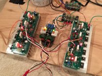
Which once laid out on the PCB out looks a bit like this:
View attachment Many_Tiny_PCB.pdf
Note 1: I was making this PCB in my shed, and considering that the board is 245mm long by 70mm wide, I did not want to be doing a full double sided PCB. For this reason I went to some effort to get the bulk of traces onto the back of the board. If I were to get some made professionally, I would double up on the power rail and output traces. As it turns out, going single sided (with a few links) did not have a serious impact on performance.
Note 2: I went to a fair bit of trouble to minimise the loop inductance between the supply rails and combined outputs coming back - this was due to my paranoia over parasitic oscillations in the output stage. For this reason I have put the power rails down between 1206 size 10 Ohm emitter resistors. This means that the "power" rails are kind of high resitance, but the maximum current on each of these will be less than an amp, and on 8 Ohm loads only 500mA peak. The compromise on track width for the supply rails was on I was willing to make.
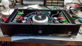
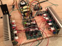
And once built (look for the wire links that are the "top layer" of the PCB):

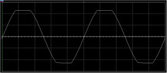
Note: that dummy load led me on a wild goose chase on distortion measurements!
As noted, distortion was a lot better than I had expected. Indeed, in my initial blog, I noted concern that Douglas Self would kick me somewhere delicate for defiling the blameless topology with this implementation!
Distortion measurements, plots are (1) loopback on the distortion test set (2) no load distortion of the "Amplifier of 100 Transistors" and (3) distortion into 8 Ohms.


There is a reasonable amount of discussion in my blog about some of the reasoning as to what I did and why, feel free to read that.
I am more than happy to post the ALTIUM files for those wishing to give this a spin. Comments though:
- I can't guarantee you won't go mad soldering on the 104 emitter resistors (SMD), the 104 base stopper resistors (SMD), 104 output devices (TO-92)
- I had no trouble with stability. Was I lucky? You will need to try and make your own call on this.
- I used BC548/558's from a single batch. (A bit like a single vineyard Shraz?) I would recommend you try not to mix and match output devices too much in a single amp.
Your challenge:
- Tweak that two pole compensation
- Try different "Output Devices" - the USA seems to favour 2N3904/6 I have not tried these, and you might want to take a look at the HFE before you jump in too far!
- If you find higher voltage devices, push the limits... Remember to tune the SOAR protection though!
- Simply build one "because you can". 10 Watts is actually enough to be useful.
Anyway, I hope this inspires someone to try something completely different for a change... have fun!
The idea of an amplifier comprised completely of small signal devices struck me, and the thought stuck - anything so silly just had to be tried. Unfortunately the idea did not leave my head until I had designed the layout, and then it was just too late and it had to be built!
Not only did the implementation work, but on testing it actually worked quite well: http://www.diyaudio.com/forums/blog...od-performance-amplifier-100-transistors.html --> not world beating, but creditable.
I have had a few comments on the BLOG for this, and I figured it might be of passing interest to "Solid State Amplifier people". This is solid state in the purest way! What other amplifier has so many output devices - and yet outputs only 10 Watts? That said however, it does so with rather unique style and in a way that I have not seen before. (Nor, may you think, should we ever see again!)
For those of you looking for the "car chase":
- The amplifier comprises ONLY BC548/558 (and in the input 549/559
- There are 54 pairs of output devices
- The amplifier runs off +/-15 Volts (VCEo for BC558 is 30 volts)
- The amplifier is a very standard blameless design
- The amplifier includes 2 slope SOAR protection, so is reasonably safe into pretty much any load
- The amplifier can happily drive 4 Ohm loads without any protection kicking in
Distortion is surprisingly low, even though I have not gone to any super effort to tune anything.
Freq No load 8R
200Hz 0.0003% 0.0003% (noise floor)
500Hz 0.0003% 0.0003% (noise floor)
1000Hz 0.0003% 0.0006%
2000Hz 0.0006% 0.001%
5000Hz 0.0015% 0.0025%
10000Hz 0.0025% 0.0044%
So what is it? Lots and lots of very low cost transistors, really. Oh, and NO heat-sink! NOTE: This schematic includes two pole compensation. The one I built has only the 120pF cap - this is the only difference between these schematics and what I built.
******* Watch out the 4K7 on the emitters of the LTP is rubbish and should be deleted or made quite a low value.
View attachment Many_Tiny_Sch_1.pdf
And the rest of the "output stage"
View attachment Many_Tiny_Sch_2.pdf
Which once laid out on the PCB out looks a bit like this:
View attachment Many_Tiny_PCB.pdf
Note 1: I was making this PCB in my shed, and considering that the board is 245mm long by 70mm wide, I did not want to be doing a full double sided PCB. For this reason I went to some effort to get the bulk of traces onto the back of the board. If I were to get some made professionally, I would double up on the power rail and output traces. As it turns out, going single sided (with a few links) did not have a serious impact on performance.
Note 2: I went to a fair bit of trouble to minimise the loop inductance between the supply rails and combined outputs coming back - this was due to my paranoia over parasitic oscillations in the output stage. For this reason I have put the power rails down between 1206 size 10 Ohm emitter resistors. This means that the "power" rails are kind of high resitance, but the maximum current on each of these will be less than an amp, and on 8 Ohm loads only 500mA peak. The compromise on track width for the supply rails was on I was willing to make.
And once built (look for the wire links that are the "top layer" of the PCB):
Note: that dummy load led me on a wild goose chase on distortion measurements!
As noted, distortion was a lot better than I had expected. Indeed, in my initial blog, I noted concern that Douglas Self would kick me somewhere delicate for defiling the blameless topology with this implementation!
Distortion measurements, plots are (1) loopback on the distortion test set (2) no load distortion of the "Amplifier of 100 Transistors" and (3) distortion into 8 Ohms.
There is a reasonable amount of discussion in my blog about some of the reasoning as to what I did and why, feel free to read that.
I am more than happy to post the ALTIUM files for those wishing to give this a spin. Comments though:
- I can't guarantee you won't go mad soldering on the 104 emitter resistors (SMD), the 104 base stopper resistors (SMD), 104 output devices (TO-92)
- I had no trouble with stability. Was I lucky? You will need to try and make your own call on this.
- I used BC548/558's from a single batch. (A bit like a single vineyard Shraz?) I would recommend you try not to mix and match output devices too much in a single amp.
Your challenge:
- Tweak that two pole compensation
- Try different "Output Devices" - the USA seems to favour 2N3904/6 I have not tried these, and you might want to take a look at the HFE before you jump in too far!
- If you find higher voltage devices, push the limits... Remember to tune the SOAR protection though!
- Simply build one "because you can". 10 Watts is actually enough to be useful.
Anyway, I hope this inspires someone to try something completely different for a change... have fun!
Last edited:
Elektor did something similar with a bunch of 5532 OPAMPs which might interest you
5532 Opamplifier Deel 1 ontwerp, filosofie en schemas
in Dutch but schematics are understandable in any language 🙂
5532 Opamplifier Deel 1 ontwerp, filosofie en schemas
in Dutch but schematics are understandable in any language 🙂
Member
Joined 2009
Paid Member
Great job - I'm glad somebody finally did this as I've had a similar idea for several years but never actually made it. Mind you, I was thinking a heatsink and Class AB would be handy to allow higher power level. I hope you are going to put this in a box and press it into service.
Last edited:
Bigun,
I am not sure how I would heatsink this other than use free air... I guess I could have used TO-126, but then that would have been cheating on the original design brief.
I do need to put it in some sort of a box. Given the TO-92's are essentially the heatsink themselves, and in a real sense are the "point" of this thing, I think they will need to be either external or rather exposed.
I have not actually listened to these yet - the measurements do suggest that it will be rather blameless in sound though!
No prizes for guessing the designer of that amplifier either....Mr Blameless, himSelf 😉Elektor did something similar with a bunch of 5532 OPAMPs......
On the topic of multiple discrete transistor amplifiers - I think Nelson Pass has taken the prize for crazy numbers of T092 parts with this one using more than 2000 JFETs! Now that's a monument to a vanishing device type: http://www.firstwatt.com/pdf/art_beast.pdf
Pass did a class A with 1000 TO92 JFETs.
http://www.firstwatt.com/pdf/art_beast.pdf
Edit : above post already caught this.
I like this because 100 is much easier to solder and the parts are not as exotic as the ones Pass uses.
http://www.firstwatt.com/pdf/art_beast.pdf
Edit : above post already caught this.
I like this because 100 is much easier to solder and the parts are not as exotic as the ones Pass uses.
Last edited:
Elektor did something similar with a bunch of 5532 OPAMPs which might interest you
5532 Opamplifier Deel 1 ontwerp, filosofie en schemas
in Dutch but schematics are understandable in any language 🙂
If this is Douglas Self's Op-Amplifier (two-part article in Elektor) then this is exactly what I was thinking of when I saw this thing. Self's project was pretty darn good and used op-amps (64?). This inspired me to do the same in my own 5532 headphone amplifier project and I measured very low THD, etc. with many devices in parallel into a 32R load (min headphone load).
Even with the base stoppers, your output stage ft should be pretty high. I'd bet you can pull down that 20k thd with some tweaking of the dominant pole compensation.
Fun, ridiculous project, I approve. 🙂
Fun, ridiculous project, I approve. 🙂
I have never seen the nelson pass device - something to behold. I do like the idea that he contracted out the tedium of soldering all the devices. But 1000!!! Wow, I need to do a bigger one!
Odd that to do something as out there as this takes inspiration from your childhood.
On the topic of getting that 20k THD down, I have no doubt whatsoever that it can be improved. My "in the head" calcs on the impact of the base stoppers suggest the output stage will still have an ft in the 10s of MHz region. I was willing and ready to use something larger than 100 Ohms if the thing took off in the RF region.
The only misbehaviour appeared to be negative rail injection back into wither the VAS or earlier, and was dealt with by using a rather large R in a negative rail RC filter for the input stage. (47 Ohms, 47uF).
I think with some time and effort this would make a very low distortion amplifier across the entire audio range. And a nice foot warmer for those cold winter afternoons we are getting down here!
The only misbehaviour appeared to be negative rail injection back into wither the VAS or earlier, and was dealt with by using a rather large R in a negative rail RC filter for the input stage. (47 Ohms, 47uF).
You could try to connect the compensation cap according to a scheme D. Self described and used : at the emitter of P6 instead of its collector.
Hi Guys
Despite the fact the output devices are types that do not bolt to heat sinks, there is still the same amount of heat to manage as a conventional 10W PA. The same goes with using parallel opamps.
3ppm at 10W is okay for some but not exactly state-of-the-art, especially when this figure is only held to 1kHz or so and THD10 is 44ppm. This is the same shape of THD vs. frequency that all of Self's amps have because he insists on miler compensation. His OIC amp has lower THD overall but still the familiar shape. I suspect there is also a topological issue since the fully-complementary amps can maintain low THD over a wider bandwidth.
Have fun
Right, the "issue" is in the front-end. This output stage deserves a better front-end topology. One of the ways to go - "current drive". Wider open loop bandwidth and no miller compensation (light lead + shunt instead).
A few examples, if I may... a simple single-end-drive and more advanced symmetric one.
Cheers,
Valery
A few examples, if I may... a simple single-end-drive and more advanced symmetric one.
Cheers,
Valery
Attachments
Valery,
Interesting thoughts on the input stage. I am getting that feeling of having gone down a rabbit hole here - and not one that I was looking to enter just now! I am getting worried that I will be spearing off into going back into alternative front end topologies - something I suspended playing with over a decade ago. Mainly because my test gear could not measure below 0.003% with any reliability, and at that time I concluded that was "good enough".
Given the point of this amplifier was as much fun and an experiment to see if the hypothesis that you COULD build a useful amplifier with just small signal transistors was true or not, it scares me that I am feeling drawn into some deep thinking on topologies again... Damn the "Amplifier of 100 Transistors"!
Way back in the past I played with fully differential front ends. I also played with current drive - though I doubt I retain any prototypes / designs as the early ones were back in the 90's.
My luck with shunt capacitors to ground (and all manner of other points) was limited, and I found that grounding became not only a signal integrity concern, but also one of RF stability of the amplifier. How have you gone with this?
Looking at the single ended current driven VAS, conceptually in my mind you are "flipping" the VAS from being common emitter to a common base, and using Q15 as a current drive (multiplied by 5.6) from the diff pair into Q3.
How well dos this work?
I would have thought you still have the option of using a miller like dominant pole back into the differential pair. Is there a reason why this is inferior to a shunt to a "signal earth" - which itself is a source of noise / injection into the output stage.
Oh and in the spirit of this thread: And how well do you reckon it would work if you used ONLY BC549/559's 😉
Well... current drive is a completely "different world".
In general, OpAmp topology designers are pretty much used to it.
It order to get familiar with the concept, you need to go away from "traditional" topologies (common emitter cascades).
Overall approach is the following:
1) V-to-I conversion in the input LTP (well degenerated);
2) Current scaling with common base / current mirrors / controlled CCS cascades;
3) I-to-V conversion via controlled CCS (current subtraction or current addition).
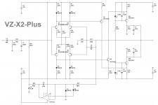
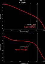
This approach gives high speed, linearity and phase of the open loop circuit, ensuring good stability margins with the global loop closed - see the feedback return ratio plots. The first one corresponds to the 1-st single-end-drive schematic (VHex+) - this is a commercially successful design (attached are the pictures of our reference build and xrk971's build). It's also showing very clean clipping behavior (see the last picture). It sounds fantastic.
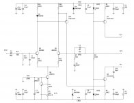
The second plot shows the feedback loop magnitude and phase curves for a more comprehensive symmetric design. Note the value (~35db) and the bandwidth (>20KHz) of the loop gain plot. The idea can be developed even further - see my "four wheel drive" topology here:
VZ-X4 front-end
No need for Miller cap whatsoever. Well, you can add it to slow down the step response, if you like 😛 How does a 56pF capacitor influence she signal integrity or inject any noise into the output stage? It acts pretty much above the audio bandwidth.
BC549/559 - no problem. Just parallel some of them in place of TO-126 devices, so that they can work at roughly 5.5mA safely.
Long tail current is 2.6mA (1.3mA per Q2, Q5 collector), Q15, Q1, Q3 all work at 5.3mA collector current.
Let me know if you will have questions.
Cheers,
Valery
In general, OpAmp topology designers are pretty much used to it.
It order to get familiar with the concept, you need to go away from "traditional" topologies (common emitter cascades).
Overall approach is the following:
1) V-to-I conversion in the input LTP (well degenerated);
2) Current scaling with common base / current mirrors / controlled CCS cascades;
3) I-to-V conversion via controlled CCS (current subtraction or current addition).
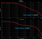
This approach gives high speed, linearity and phase of the open loop circuit, ensuring good stability margins with the global loop closed - see the feedback return ratio plots. The first one corresponds to the 1-st single-end-drive schematic (VHex+) - this is a commercially successful design (attached are the pictures of our reference build and xrk971's build). It's also showing very clean clipping behavior (see the last picture). It sounds fantastic.
The second plot shows the feedback loop magnitude and phase curves for a more comprehensive symmetric design. Note the value (~35db) and the bandwidth (>20KHz) of the loop gain plot. The idea can be developed even further - see my "four wheel drive" topology here:
VZ-X4 front-end
No need for Miller cap whatsoever. Well, you can add it to slow down the step response, if you like 😛 How does a 56pF capacitor influence she signal integrity or inject any noise into the output stage? It acts pretty much above the audio bandwidth.
BC549/559 - no problem. Just parallel some of them in place of TO-126 devices, so that they can work at roughly 5.5mA safely.
Long tail current is 2.6mA (1.3mA per Q2, Q5 collector), Q15, Q1, Q3 all work at 5.3mA collector current.
Let me know if you will have questions.
Cheers,
Valery
Attachments
+1 - I can attest that the current drive works wonderfully - the amp Valery designed is one of my best sounding amps. 🙂
It's great to see the topology explained step by step above. It's not that hard to build actually - I think the above design (SE on left) was taken straight from the current VHex+ amp which requires rather HV components for the 50v rails on the IRFP240 and 9240 OPS. But for smaller rail voltages you can go with lower cost easier to find BD139/140's or even maybe smaller TO92's - maybe Valery can give suggestions that would be well matched for the 100 transistor output stage. But then again driving 100 bases may require some current so a TO126 is not surprising.
It's great to see the topology explained step by step above. It's not that hard to build actually - I think the above design (SE on left) was taken straight from the current VHex+ amp which requires rather HV components for the 50v rails on the IRFP240 and 9240 OPS. But for smaller rail voltages you can go with lower cost easier to find BD139/140's or even maybe smaller TO92's - maybe Valery can give suggestions that would be well matched for the 100 transistor output stage. But then again driving 100 bases may require some current so a TO126 is not surprising.
Last edited:
Member
Joined 2009
Paid Member
Bigun,
I am not sure how I would heatsink this other than use free air... I guess I could have used TO-126, but then that would have been cheating on the original design brief.
I do need to put it in some sort of a box. Given the TO-92's are essentially the heatsink themselves, and in a real sense are the "point" of this thing, I think they will need to be either external or rather exposed.
I thought a heatsink would have been good, with TO-126. But what you did is even more fun. Maybe use a box, power supply inside box, pcb of the amp mounted on top like a tube amp
alternative front end topologies
Refinements in the standard long tail pair topology are promising :
see figures 48 and 50 of
http://www.nanovolt.ch/resources/power_amplifiers/pdf/audio_power_amp_design_comments.pdf
- Status
- Not open for further replies.
- Home
- Amplifiers
- Solid State
- The Amplifier of 100 Transistors - Blameless using small signal devices as outputs!