iwahn,
I posted 2 PCBs, the first one, has errors, but the second I was pretty sure about. and as it has been downloaded about 150 times I would have thought(hoped) that someone would have spotted the any errors and mentioned it??
I would have removed the earlier version if I could.
sorry for any inconvenience.
I haven't been able to get any IRF9610s yet, I am a little perturbed by the fact that I can get a tube of 50 for about Aust$20 more than I would pay for a lot of 10 and a few other sources seem to have dried up since the printing of their catalogues and the present.
James
Member
Joined 2002
James can you send me them schematics and pcb files please thanks
Jason
jleaman@citytel.net
P.s Mabey all the paper work if you have it i want to try it i have lots of part i think tha ti can put one together too..
Jason
jleaman@citytel.net
P.s Mabey all the paper work if you have it i want to try it i have lots of part i think tha ti can put one together too..
does it work?
This is not a completly debugged design. I wolud not reccomend that anyone build it without a pretty good amount of experience with amplifiers. Perhaps it was premature to post a schematic till it is built and tested.
H.H.
This is not a completly debugged design. I wolud not reccomend that anyone build it without a pretty good amount of experience with amplifiers. Perhaps it was premature to post a schematic till it is built and tested.
H.H.
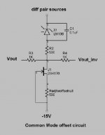
Offset Null Circuit for Aleph X
Harry, your idea is similar to one I mentioned in a (now rather old) previous post.
It is a nice idea and I see that yours is different from mine in the addition of R1. However, to some extent are you not just moving the problem elsewhere? If the current from I1 is not exactly correct, will it not create its own, unwanted DC offset?
Ian.
Harry, your idea is similar to one I mentioned in a (now rather old) previous post.
-- Vgs matching
Regarding my use of a MOSFET for Vgs compensation with the common mode feedback resistors. I take your point about not being able to match the value due to the difference in current between driver currents and compensation voltage source. In fact I don’t think the idea is really practical, at least not as I had it. The current in the MOSFET acting as a voltage source is far too low (tens of microamps) and varies with a consequent effect on Vgs. In theory this could be rectified by the addition of another current source between the junction of R87 and R89 (as per my last post) and the negative power supply. However, in practice there would be a similar problem of determining this current accurately enough and it all gets too complicated.
It is a nice idea and I see that yours is different from mine in the addition of R1. However, to some extent are you not just moving the problem elsewhere? If the current from I1 is not exactly correct, will it not create its own, unwanted DC offset?
Ian.
Offset null
No..... I think we are talking about different points. The idea is the keep the juction of the common mode feedback resistors ( between the outputs and input sources junction) at a zero volt point so as not to dump AC current into the sources of the front end diff pair. The circuit adds a DC offset to this junction to match the gate to source voltage of the input mosfet diff pair. DC feedback is still there, but no AC current into sources. Go put a few different values of output voltages and the opposite polarity of voltage on the other output and you will see currents into the sources due to the DC offset of about 3 volts the junction of the input sources relative to the 0 volt average of the the output voltages (as they swing differeny polarities from each each other with the same amplitude.)
H.H.
Offset null
I beg to differ (in terms of talking about the same thing) - I think we were both trying to address the same problem 🙂 Probably I wasn't sufficiently clear and I did rather quote out of context. Anyway, enough excuses from me.
I still think that you may have a potential problem with DC offset produced by the addional current source if it does not produce precisely the right value, but perhaps I have an exagerated impression of the effect. I'll have to get the old simulator out again...
Ian.
For guys who can adjust it themselves occasionally, or who
don't worry about a fraction of a volt, it's overkill.
From a manufacturing standpoint, you want
low absolute values because some offshore customer
will measure this and get excited when it's .5 volts or so,
and they don't believe that a quality product should allow
such sloppiness.
don't worry about a fraction of a volt, it's overkill.
From a manufacturing standpoint, you want
low absolute values because some offshore customer
will measure this and get excited when it's .5 volts or so,
and they don't believe that a quality product should allow
such sloppiness.
offset circuit
Any real advantage to the Vgs offset for the common mode feedback resistors to the sources Mr.Pass?
H.H.
Any real advantage to the Vgs offset for the common mode feedback resistors to the sources Mr.Pass?
H.H.
Have tested the channel that responded to adjustments.
As long as I have only one channel, it´s difficult to give a good description of the sound, but my impression is that the circuit gives a clear and detailed reproduction. A higher outputlevel brings some distortion, possibly due to the fact that my psu only delivers 10 volts to the rails. The conclusion must be that Greg´s efforts have been very succesful. Regarding the other channel buildt on the pcb provided by James, I guess the problems I described in my previous post, is the result of failure in a component. Any sugestions about what the error could be, is highly regarded as my knowledge in elecronics is somewhat limited compared with the majority in this forum.
As long as I have only one channel, it´s difficult to give a good description of the sound, but my impression is that the circuit gives a clear and detailed reproduction. A higher outputlevel brings some distortion, possibly due to the fact that my psu only delivers 10 volts to the rails. The conclusion must be that Greg´s efforts have been very succesful. Regarding the other channel buildt on the pcb provided by James, I guess the problems I described in my previous post, is the result of failure in a component. Any sugestions about what the error could be, is highly regarded as my knowledge in elecronics is somewhat limited compared with the majority in this forum.
Pretty Solid
I agree, your CM offset null circuit is pretty solid. However, I also feel (in keeping with both you and Nelson I think) that it is probably overkill, i.e. is the problem it solves really a problem at all? The performance of the circuit with and without the Vgs correction does not appear to be that different and the adjustment on the diff pair current source will still be required. It might be worth noting though that the ‘problem’ is considerably reduced if a JFET input stage is used…
Ian.
reduced if a JFET input stage is used
The diffential offset wound be reduced but you will have the same
common mode offset effect for the same given current source for the front end. Stability of the current source is very important if the offset is not to drift with temperature and power supply voltage. That is why I am using a voltage reference and fet current source to bias it instead of a zener and resistor. For those comptemplating a jfet front end be aware the jfet doesn't have as high a transconductance as the mosfet front end and the drain resistor will have to be higher for the same open loop voltage gain. This will increase high frequency distortion and reduce bandwidth for the amp. The aleph front end and output are a much more synergistic combination than one would think at first glance.
H.H.
Current Source Bias
Just to clarify, I was talking about the Vgs offset being smaller (and opposite in polarity) for the JFET front end. I realise that the common mode offset is critically dependent on the input current source stability.
I'm a little confused by your comment about alternative bias for the current source - are you referring to your recent post? I thought this subcircuit was connected to the sources of the input MOSFETs rather than the gate of the current source. Can you clarify please? BTW, I completey support the idea of stablising the current source as much as possible - this will have benefit for both the DC and AC common mode output.
Regarding your comment about replacing front end with JFETs. I reduced the value of the current by approx half and doubled the drain resistors. The (simulated) frequency response using J109 actually improves over the MOSFET front end and rolls off more gently. I'll publish the traces when I'm back at home.
Ian.
Current source reference
My reference to current source bias is for a fixed current source such as that for all the aleph amp front ends. The tempco for a zener and the variation in zener voltage with varying supply voltage is probably not optimum for a very stable current source. For lower value supply rails this becomes more of an issue as the resistor becomes small for the same bias current through the 9 volt zener. With Grey's value of 1.5K to bias a 9V zener from a 15 volt supply, I would estimate that the zener voltage will change about 10 millivolts for every volt change in supply voltage.
I believe the dominant pole is the drain resistor for the front end and the gate to souce capacitance of the output stage mosfets. You are moving this pole away other poles in the response of the amp which gives a smoother roll off. I believe you are also reducing the open loop gain of the amp increasing output impedance and distortion due to less open loop gain. The ZEN articles discuss the effect or souce impedance on high frequency distortion for the common source mosfet gain stage and are well worth reading for insight into this distortion mechanism. As always thanks for your very learned input. What Spice simulator are you using so we can compare and maybe swap device models?
H.H.
Current source reference
Thanks for trying to clear my confusion. If I understand you correctly, you are using the same bias scheme for the front end tail current source as you posted for DC offset null purposes, i.e. same scheme – different application. Am I correct in assuming your primary focus here is DC (static) stability in the face of temperature and/or supply voltage variations? I ask since the obvious alternative is the typical two transistor/MOSFET technique in a feedback scheme. This would of course also affect the dynamic performance of the current source. Do you see the latter as a problem or is there another reason to prefer the single device current source?
You make an interesting point about the dominant pole of the Aleph-X circuit – not something I have yet investigated. My intuition tells me you are probably right though, seeing as how the high frequency response is so strongly influenced by the impedance of the driver. In addition, the frequency response traces seem to support the theory (see attached). I am less sure about the reduced open gain – surely the larger driver drain resistors will tend to compensate for the lower transconductance of the JFETs? In any case I see no increase in simulated distortion, though I don’t much trust this aspect of Spice simulators. I didn’t think to try and measure output impedance with this modification, but will have a go shortly.
Spice simulators – now that’s a thorny topic. Most that I have encountered are not all that good or else they are way too expensive. CircuitMaker has a nice user interface but its simulation ability is not in the same league, e.g. it doesn’t cope well with current sources and will frequently fail to converge on a solution at all. I wasted my money on a copy of EDSpice some time ago and it has proved of no use to me at all. I am currently using a student version of Pspice (from Orcad). This has an inferior user interface (compared with CircuitMaker) but does a much better job of simulating things accurately. Unfortunately I cannot afford the commercial version. The student version has too few models and imposes a small limit on the number one can import/create. If you know of anything better that is available at a reasonable price (I would be willing to pay two to three hundred dollars) then please shout! Compare and swap device models? By all means though I doubt that I have much that would interest you.
Ian.
Attachments
Ian,
do you know anything about Electronics Workbench?
I know I student edition can be obtained for very little cash. I was going to get it but since I don't know anything about it I really don't want to blow 70 dollars.
do you know anything about Electronics Workbench?
I know I student edition can be obtained for very little cash. I was going to get it but since I don't know anything about it I really don't want to blow 70 dollars.
Electronic Workbench
I have no personal experience of EW. However, I believe it is now rather old and has been superceded by Proteus VSM. Others have said that they don not trust its simulations but I don't know on what this opinion was based.
Ian.
I have no personal experience of EW. However, I believe it is now rather old and has been superceded by Proteus VSM. Others have said that they don not trust its simulations but I don't know on what this opinion was based.
Ian.
EWB is a very nice piece of software but to get the professional version costs many thousand dollars last time I checked and since the student version isnt worth its wait in salt, I find myself looking elsewhere.
Re: Current source reference
Ian:
Have you evaluated SwitcherCAD III (free download) from Linear Technology? Weak on models, but sem sto be fairly capable.
mlloyd1
Ian:
Have you evaluated SwitcherCAD III (free download) from Linear Technology? Weak on models, but sem sto be fairly capable.
mlloyd1
Ian Macmillan said:Spice simulators – now that’s a thorny topic. Most that I have encountered are not all that good or else they are way too expensive. ...If you know of anything better that is available at a reasonable price (I would be willing to pay two to three hundred dollars) then please shout! ....Ian.
- Home
- Amplifiers
- Pass Labs
- The Aleph-X