All uploaded pictures, videos, schematics and board layouts of "my" amp have been deleted.
That would blow out 99% of the Solid State forum content if everyone followed suit...
Nothing wrong with a fresh look at an established design.
Ok i reuploaded some of the pics and schemos and layouts under "basedonblameless" as not to hurt copyrights as much as "of my own design" did.
In fact its only bootstrapping and the use of laterals and no bias transistor that differ my project from rod elliott's P101, other than that its identical.
In fact its only bootstrapping and the use of laterals and no bias transistor that differ my project from rod elliott's P101, other than that its identical.
When told that the circuit is based on the blameless, I thought you had the book and knew the circuit, there are amplifiers commercial that use circuit similar, as the Mark Levinson and Luxman.Ok i reuploaded some of the pics and schemos and layouts under "basedonblameless" as not to hurt copyrights as much as "of my own design" did.
In fact its only bootstrapping and the use of laterals and no bias transistor that differ my project from rod elliott's P101, other than that its identical.
Use resistors degenerative for linearity with mosfets do search on the subject, Bob Cordell did research and measurement at Mosfets. After done, your circuit will authentic certainly, or rename the amp for "Frankenstein"

Last edited:
Not just that ,but the sine gen. in spice generates .005% just by itself.
I don't think so 😀
Attachments
Ok i reuploaded some of the pics and schemos and layouts under "basedonblameless" as not to hurt copyrights as much as "of my own design" did.
In fact its only bootstrapping and the use of laterals and no bias transistor that differ my project from rod elliott's P101, other than that its identical.
Probably half the amps designed in the past 30 years are as close to the blameless as you are. The differences are in the details, and thats what makes them sound different. These details also turn an ordinary LTP/CE VAS/double (triple) Emiter folower output amp into a very low distortion blameless amp.
New amplifiers that dont rely on old stage designs that are tweaked are extremely rare. (reinventing the wheel is great education, but thats about it) So dont worry about stealing ideas, especialy if its for DIY.
Elvee:
Are you saying your amp has zero distortion?
Very low anyway, by the looks of it. The chart is hiding the circuit - must be top secret!
🙂
The high end of the gain from 100kHz and up looks like that because i put it at the verge of wanting to oscillate.
The phase prollems i dunno if there is a cure for since i normally don't work with discrete class AB.
The phase prollems i dunno if there is a cure for since i normally don't work with discrete class AB.
It does, but it also increases THD to 0.005% and above
The phase prollems are likely since this circuit was intended to drive bipolars, not mosfets.
The phase prollems are likely since this circuit was intended to drive bipolars, not mosfets.
It does, but it also increases THD to 0.005% and above
The phase prollems are likely since this circuit was intended to drive bipolars, not mosfets.
You need to study the loop gain and phase margin.
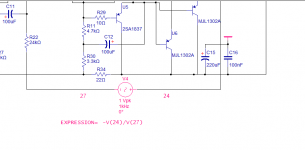
Ground the input and insert an AC signal source in the feedback loop:

Find the nets before and after the signal source and plot the expression -V(before)/V(after) on an AC analysis.
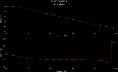
You'll get a result like this:

This shows loop gain at the top, phase at the bottom. Notice when the LG hits 0, the phase should optimally be -100 degrees.
If you take a look in the LTSpice examples folder, there is the 'Middlebrook' procedure for extracting the LOOP GAIN/PHASE. You need look at LOOP GAIN/PHASE to judge the stability of your amplifier and to compensate it correctly. A closed loop plot does not give the true story - you need to be really experienced to judge an amplifiers stability from the closed loop gain and phase, and what to do to optimize it.
Part of the art of compensation is making the correct performance tradeoff's to acheive optimum stability at the best possible performance (=lowest distortion, adeqaute slew rate).
My suggestion is that you use the LTSpice tool mnetioned above, re-run your simulation and then post the results up.
Some ideas to think about:-
1. Your tail current is far too low (<1mA). Run it at 3mA to 10mA (10mA is where I run mine, but some would say this is too high).
2. Your LTP degeneration resistors are too low at 22 Ohms. They probably need to be 50 ohms or more to ensure adeqaute slew rate and avoid TIM.
3. The LTP current is also too low and is easily modulated by the output load and cross over switching. I would run this at a minimum of 10mA, although I run my designs at about 30mA.
4. Also, Q3 needs some degeneration - use about 33 Ohms here (you can optimize this empirically on LTSpice).
5. Your gate stopper resistors are on the low side - I'd fit something like 50 Ohms.
6. I'd also fit an output inductor of around 1uF, and a Zobel network (junction of R10 and R11to 0V return where the filter caps join).
Mosfets are fast, so you can get away with greater loop gains, but heavy capacitive loads are still an issue and can lead to stability problems.
Last edited:
Looks like you beat me too it MJL21193.
🙂
TBH, I'm a bit rusty, long out of the loop (pun!) and had to really work my brain to remember.
These things I forget too easily.
- Status
- Not open for further replies.
- Home
- Amplifiers
- Solid State
- THD in LTSpice ?


