As a DIY challenge, I followed for my Main Amp a route where gain and power were split over resp. a very fast low power 27.5dB voltage amplifier followed by a separate 0dB buffer.
I’ve seen others doing the same like Jan Didden around a AD844 and LKA with discrete transistors.
They both used the so called Hawskford Error Correction or HEC.
HEC implementation is an (active) error correction principle around a 1x gain correction stage that subtracts the difference between input and output from the input.
This can theoretically reduce all distortion, but practical designs do need very precise tuning and a very careful choice of topology.
It cannot compensate the distortion caused by the input adder and neither does it correct the Amp’s output offset.
There are other Active Error Feedback principles, with more flexibility not needing any tuning at all and at the same time taking control of the Amp’s output offset voltage.
The most simple version is called FDR (feedback distortion reducer) that only needs one op-amp, a resistor and a bandwidth limiting cap around said op-amp.
In case of a high voltage buffer, this op-amp asks for a floating supply driven by the Amp’s output. But there's more to reduce distortion as will be discussed.
The 4 versions will be shown in four postings, so here's the first one.
Version 1
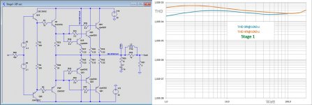
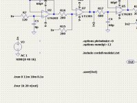
The first version in this thread is a straightforward 3 stage buffer, equipped with modern transistors taken from the Cordell models.txt library, such as often used on this DIYAudio forum, nothing special, but perfectly suited for the purpose of this thread.
Idle current chosen was slightly below 300mA, giving a flat FR from a low impedance source.
In the attached image the circuit diagram is shown for the used buffer, together with its THD for 8R and 4R @ 10Khz versus power from 1Watt to resp. 100Watt and 200Watt for both loads.
Idle current in one of three output transistors, as well as the output offset voltage are visible in the diagram.
THD lies between 0.1% and 0.01%.
Hans
Addendum: Distortion figures presented in my images are not to be confused with percentages.
So 1e-2 = 1%, 1e-4 = 0,01% etc.
With the same logic, 1ppm is 0,0001% or -120dB.
I’ve seen others doing the same like Jan Didden around a AD844 and LKA with discrete transistors.
They both used the so called Hawskford Error Correction or HEC.
HEC implementation is an (active) error correction principle around a 1x gain correction stage that subtracts the difference between input and output from the input.
This can theoretically reduce all distortion, but practical designs do need very precise tuning and a very careful choice of topology.
It cannot compensate the distortion caused by the input adder and neither does it correct the Amp’s output offset.
There are other Active Error Feedback principles, with more flexibility not needing any tuning at all and at the same time taking control of the Amp’s output offset voltage.
The most simple version is called FDR (feedback distortion reducer) that only needs one op-amp, a resistor and a bandwidth limiting cap around said op-amp.
In case of a high voltage buffer, this op-amp asks for a floating supply driven by the Amp’s output. But there's more to reduce distortion as will be discussed.
The 4 versions will be shown in four postings, so here's the first one.
Version 1
The first version in this thread is a straightforward 3 stage buffer, equipped with modern transistors taken from the Cordell models.txt library, such as often used on this DIYAudio forum, nothing special, but perfectly suited for the purpose of this thread.
Idle current chosen was slightly below 300mA, giving a flat FR from a low impedance source.
In the attached image the circuit diagram is shown for the used buffer, together with its THD for 8R and 4R @ 10Khz versus power from 1Watt to resp. 100Watt and 200Watt for both loads.
Idle current in one of three output transistors, as well as the output offset voltage are visible in the diagram.
THD lies between 0.1% and 0.01%.
Hans
Addendum: Distortion figures presented in my images are not to be confused with percentages.
So 1e-2 = 1%, 1e-4 = 0,01% etc.
With the same logic, 1ppm is 0,0001% or -120dB.
Attachments
Last edited:
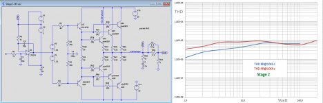
Version 2
The second version shows the same buffer where the first stage has been replaced by an op-amp with floating supply.
THD has been significantly reduced almost by a factor 50 in the high 1 digit ppm region, showing the ease how FDR (Feedback Distortion Reduction) can substantially reduce THD and output offset voltage at the same time.
Hans
Attachments
Version 3
The non linear behaviour of the power transistors is further taken care of by giving the positive and the negative half an additional op-amp to linearise these 2 halves.
In combination with the FDR solution of stage 2, distortion has now been reduced by another factor of 3 and is in the low 1 digit ppm region.
But there's even more to come, with a nested feedback topology in version 4.
Hans
Attachments

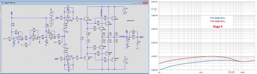
Version 4
This is the most sophisticated version, having nested feedback of two active error feedback stages, with a buffer in between for stability reasons.
A bit more complex as in stage 2 and 3, but with an enormous open loop gain, stability at start up should be guaranteed.
As can be seen, THD now is between 0.01 and 0.1 ppm for all input voltages at 10Khz.
10Khz is very demanding when testing an Amp, but for audio it is less important because the rather harmless H2 is at 20Khz, already outside our hearing ability.
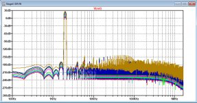
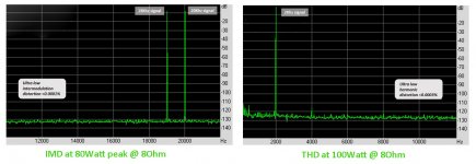
Now going to 2Khz with this version 4 brings all simulated distortion way below 0,01 ppm or -140dB, see FFT spectra for all voltages at 4R load in the second image below.
This is a hypothetical THD level as produced by LTSpice that goes beyond practical limitations, but a real life 80Watt 19&20 Khz IMD distortion and a 2Khz 100Watt measurement gave the results in image 3.
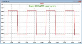
In the fourth image a rather impeccable 10Khz square wave is shown.
After having used this version 4 over the last 5 years, I can say that it works without a single flaw.
Hans
This is the most sophisticated version, having nested feedback of two active error feedback stages, with a buffer in between for stability reasons.
A bit more complex as in stage 2 and 3, but with an enormous open loop gain, stability at start up should be guaranteed.
As can be seen, THD now is between 0.01 and 0.1 ppm for all input voltages at 10Khz.
10Khz is very demanding when testing an Amp, but for audio it is less important because the rather harmless H2 is at 20Khz, already outside our hearing ability.
Now going to 2Khz with this version 4 brings all simulated distortion way below 0,01 ppm or -140dB, see FFT spectra for all voltages at 4R load in the second image below.
This is a hypothetical THD level as produced by LTSpice that goes beyond practical limitations, but a real life 80Watt 19&20 Khz IMD distortion and a 2Khz 100Watt measurement gave the results in image 3.
In the fourth image a rather impeccable 10Khz square wave is shown.
After having used this version 4 over the last 5 years, I can say that it works without a single flaw.
Hans
Attachments
Impressive results. The error corrector takes its reference from after the inductor. How does capacitive loading affect behavior?
The reference point for the error correction is before the inductor.
Sensitivity for capacitive loading will depend on several aspects and can best be tested on a ready made amplifier.
My amplifier driving Quad ESL speakers did not need an inductor at all.
Hans
Sensitivity for capacitive loading will depend on several aspects and can best be tested on a ready made amplifier.
My amplifier driving Quad ESL speakers did not need an inductor at all.
Hans
Very cool work. It is interesting how the conventional rail referenced long tailed pair design philosophy starts to become less attractive for unity gain outputs. I know Linear Audio has at least one article showing such an implementation. Then there are also a number of floating designs on this forum with a carefully designed stage gain to avoid clipping the different rails. It seems that floating linearization is most elegant for gain of 1 amplifiers.
By calculation, your version 3 should have a roughly 2X improved distortion rejection if I read the loop gain correctly as 1, and get 1/(1+loop gain) linear disturbance rejection. Maybe it gets 3x benefit because the distortion is nonlinear, or does it have something to do with the parallel sections?
All the same tricks should be relevant to floating amplifiers as are appropriate for fixed amplifiers. I believe one should be able to use 2nd order or output inclusive feedback in one stage and get the same net loop gain as with a nested two-stage loop. I tried the concept for one of the circuits in my related thread, and did get a simulation benefit for the cost of a single extra resistor and capacitor. My discrete formulation had a finite maximum loop gain, but your opamp version should be able to realize the full theoretical performance of a second order loop using the one stage. I wonder if this would be worth trying, or does having the independent stages provide stability benefits when each stage clips?
As an aside, how do you go about computing THD in LTSpice?
It has to do with the linearization of the output transistors.By calculation, your version 3 should have a roughly 2X improved distortion rejection if I read the loop gain correctly as 1, and get 1/(1+loop gain) linear disturbance rejection. Maybe it gets 3x benefit because the distortion is nonlinear, or does it have something to do with the parallel sections?
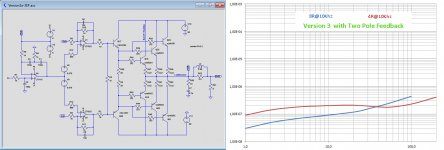
Absolutely correct. In the image below version 3 is shown with Two Pole Feedback (TPF), giving a substantial reduction of THD, not as good but close to the nested version.I believe one should be able to use 2nd order or output inclusive feedback in one stage and get the same net loop gain as with a nested two-stage loop.
But there is a very subjective reason why I skipped this.
As mentioned, I have implemented version 4 in my own Amp, after first having tried version 3 without and with TPF.
In both case THD was far below what's needed, but the sound became cold and less musical compared to the single pole feedback.
That's why I went for the nested version that did not have this side effect.
But I want to avoid with all means putting this as a general truth.
I have tried to analyse the possible reason with LTSpice, and what came out for my situation was that TPF causes a significantly longer settling time.
But if this is the cause of a sound that was perceived as worse, I have no idea, but I just choose what sounded best to my (very subjective) taste.
By inserting the "four" command in your model, then clicking on the simulated time image, followed by clicking "view" and "Spice error log".As an aside, how do you go about computing THD in LTSpice?
Finally scroll down to where you will find all THD information.
Hans
P.S. Just note that I have changed the input cap from 50pF to 100pF. This should also be changed to version 3.
Attachments
Last edited:
I tried to simulate, .lnclude cordell models1.txt , I couldnlt make it read. I adjusted the .four measurement requirements for high precision mode. Not valide for FFT. can you post the result file?
Hayk
Hayk
Attachments
Last edited:
Thank you for the tip on calculating THD.
Your experience with implementing 2 pole feedback is interesting and gives me hope I will have success with this architecture. I had implemented a 3rd order conditionally stable amplifier which oscillated for some bias settings, and when using output inclusion. The model I used to explain the findings was that crossover distortion and current limiting changes the apparent impedance and voltage divider of the feedback networks. For example, the amplifier would oscillate at a low level in an underbiased condition because the output impedance relative to the zobel was much higher than modeled and dropped the loop gain. Interestingly, adding the separate floating linearization loop stabilized the simulation by making the apparent output impedance more predictable.
I did observe in simulation that the internal drive signal (with feedback) has much greater slew rate than the output signal in the crossover region, especially in lightly biased conditions and I wonder if this has practical implications. It might be different in your case because you have a healthy standing current, and the opamps should slew pretty well. It seems you would see these effects if they did exist in the measured distortion, but maybe the music was a more challenging test signal than tones.
I was trying to explore what causes the upper allowable bandwidth limit in simulation, and found the loop gain started going back up at high frequencies. Increasing the base stopper resistor, and increasing the distributed capacitance at the predriver input improved the gain margin, but both mitigations resulted in lower overall bandwidth. I will look at the RC filter you showed in the previous post (VER2), but I was also considering one could add a lead network in the feedback in the form of R || (R+C).
Your experience with implementing 2 pole feedback is interesting and gives me hope I will have success with this architecture. I had implemented a 3rd order conditionally stable amplifier which oscillated for some bias settings, and when using output inclusion. The model I used to explain the findings was that crossover distortion and current limiting changes the apparent impedance and voltage divider of the feedback networks. For example, the amplifier would oscillate at a low level in an underbiased condition because the output impedance relative to the zobel was much higher than modeled and dropped the loop gain. Interestingly, adding the separate floating linearization loop stabilized the simulation by making the apparent output impedance more predictable.
I did observe in simulation that the internal drive signal (with feedback) has much greater slew rate than the output signal in the crossover region, especially in lightly biased conditions and I wonder if this has practical implications. It might be different in your case because you have a healthy standing current, and the opamps should slew pretty well. It seems you would see these effects if they did exist in the measured distortion, but maybe the music was a more challenging test signal than tones.
P.S. Just note that I have changed the input cap from 50pF to 100pF. This should also be changed to version 3.
I was trying to explore what causes the upper allowable bandwidth limit in simulation, and found the loop gain started going back up at high frequencies. Increasing the base stopper resistor, and increasing the distributed capacitance at the predriver input improved the gain margin, but both mitigations resulted in lower overall bandwidth. I will look at the RC filter you showed in the previous post (VER2), but I was also considering one could add a lead network in the feedback in the form of R || (R+C).
Last edited:
I tried to simulate, .lnclude cordell models1.txt , I couldnlt make it read. I adjusted the .four measurement requirements for high precision mode. Not valide for FFT. can you post the result file?
Hayk
Hi Hayk,
I made small adjustments in the names that Cordell used, a Qnjw302C was renamed in njw302 etc, etc.
After having renamed, I renamed the complete file into Cordell models1.txt see below.
I don't understand your .four adjustment, it's all there in the .asc file that you have.
When you want a higher precision, all you have to do is to change the .param FFT from 2**16 into a larger power like 2**18.
Which result file are you asking for ?
And don't forget to change the input cap from 50pF into 100pF.
Hans
Attachments
@mazurek
Still coming back on your question about the linearization of the output halves,
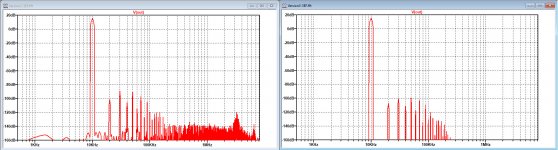
I simulated an FFT for 4R @ 10Khz at 10 Watt for versions 2 and 3.
As you may see, version 3 does not at all have all the noise above 200Khz and also the peak slightly above 3Mhz is missing.
So version 3 has more benefits than just a lower THD.
Hans
Still coming back on your question about the linearization of the output halves,
I simulated an FFT for 4R @ 10Khz at 10 Watt for versions 2 and 3.
As you may see, version 3 does not at all have all the noise above 200Khz and also the peak slightly above 3Mhz is missing.
So version 3 has more benefits than just a lower THD.
Hans
Attachments
Please have a look in some old models from Denon in the POA monoblocks line.
It was done with very similar idea using simple and cheap integrated OpAmp Like NE5534.
Good look
It was done with very similar idea using simple and cheap integrated OpAmp Like NE5534.
Good look
Last edited:
Thank you for mentioning this.
Do you happen to have more details like a circuit diagram ?
Would be interesting to see what they did.
Hans
Do you happen to have more details like a circuit diagram ?
Would be interesting to see what they did.
Hans
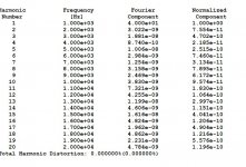
Fourier Analysis has different requirements than the FFT. To get a precise values you must study a single cycle in steady state after 1000 cycles. The single cycle is sampled by 10k points. The number of harmonics are 20 audible for 1khz. See post 35.
how to measure precisely distortion with LTspice?
how to measure precisely distortion with LTspice?
Yep. Composite amplifiers work well. 🙂 It'll be interesting to see how well the sims hold up to reality. Stability is definitely a challenge in composite amps. I recommend simulating with 8 ohm in parallel with increasing capacitance. I usually go up to 1-5 uF.
Tom
Tom
- Home
- Amplifiers
- Solid State
- THD going down from 100ppm to 1/100 ppm in 4 versions of a 100W@8R / 200W@4R buffer