excess loop gain at any frequency reduces errors measured by the negative feedback loop's error differencing input at the same frequency
increase low frequency loop gain and low frequencies harmonic distortions are reduced by the gain at the frequency of the harmonics
and more importantly low frequency IMD difference products of higher frequency multitones are reduced by the excess loop gain at the frequency of the distortion product even if the higher frequency distortions that generated them don't see more loop gain
Jcx can you clarify this
"on signal content alone it is extremely implausible that microsecond amplifier settling time is important to commercial recorded music signals that have been 4th order low pass filtered at 50 kHz or less (usually much less) by the combination of recording microphones and loudspeaker transducer's basic physics limits"
Are you referring to something like 20 kHz = 50 uS so settling time of 1 uS is irrelevant?
Last edited:
latest implementation results
Hi mates,
This is to report the latest implementation results.
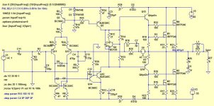
Some modifications have been made to the circuit in the opening post. Firstly, in the VAS, as zenelectro and Douglas Self mentioned, the compensation cap C12 is modified to across the whole Baxandall pair formed by Q14 and Q10. R36 is increased from 1150ohm to 33k, so that it supplies about 1.6 mA enough but not excessive bias current to the Q14 emitter. C2 and R7 are removed from the base circuit of Q14, since they neither help to eliminate the high frequency parasitics nor help the VAS recover better from clipping. The Q13 is also removed from the constant current source since it does not help here (maybe it does, but just does not show by Spice simulation). Secondly, two 100ohm emitter resistors are added to the LTP Q11 and Q12, also the emitter resistors of the current mirror is reduced from 690ohm to 47 ohm as suggested by BV. These changes, I hope, help to linearize the input stage and the VAS. And then, the output stage is changed to compound quasi complementary with Mosfet as output transistors. Reason for changing the output from bjt to Mosfet is that I want to use TO3 metal can transistors for good thermal stability and achieve good linearity at large load such as 2 to 4ohm, where current may > 10A. In viewing hfe-Ic curves of the popular TO3 bjt transistors, I have not found any good ones for this purposes. I happen to have some older 2SK313 metal cans, so I used them in the implementation. I am not sure if the old slow 2SK313 is the right choice for this amp, but it has a rated Idmax of 12A and small input capacitance, and it is designed for high frequency amplification as stated in the datasheet (see attached). For the two driver transistors, I actually use 2SA1930/C5171, which is more modern than the old fashioned TIPs.
Figure1.

The finished amp is shown in the above Figure1. I have measured the amp with since and sq wave, and listening-tested this amp with a +/-30V DC power supply. The frequency response roughly replicates the Spice simulation. I also have not implemented the low pass filter inductor L1 and R21. My scope can show frequency up to 100MHz. There is no resonance at any frequency up to 200KHz sq wave, higher frequency sq ware signal not tested. Sound is ok but nothing particular to mention. At least when there is no signal, the amp is deadly quiet.
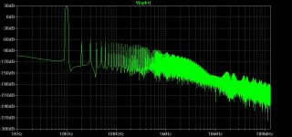
The current LTspice simulation results is 0.0053% THD at 10KHz 84vpp sine wave to 8ohm load.
Harmonic Frequency Fourier Normalized Phase Normalized
Number [Hz] Component Component [degree] Phase [deg]
1 1.000e+04 4.184e+01 1.000e+00 -2.48? 0.00?
2 2.000e+04 8.562e-04 2.046e-05 85.44? 87.92?
3 3.000e+04 1.433e-03 3.425e-05 135.12? 137.61?
4 4.000e+04 5.211e-04 1.245e-05 90.62? 93.10?
5 5.000e+04 7.201e-04 1.721e-05 -28.20? -25.72?
6 6.000e+04 9.079e-04 2.170e-05 81.75? 84.23?
7 7.000e+04 3.668e-04 8.766e-06 103.40? 105.88?
8 8.000e+04 5.804e-04 1.387e-05 84.51? 86.99?
9 9.000e+04 4.048e-04 9.674e-06 69.16? 71.64?
Total Harmonic Distortion: 0.005363%
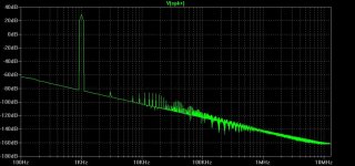
0.000298% THD at 1KHz 84vpp sine wave to 8ohm load.
Harmonic Frequency Fourier Normalized Phase Normalized
Number [Hz] Component Component [degree] Phase [deg]
1 1.000e+03 4.189e+01 1.000e+00 -0.17? 0.00?
2 2.000e+03 4.436e-05 1.059e-06 -158.28? -158.11?
3 3.000e+03 8.531e-05 2.037e-06 101.42? 101.60?
4 4.000e+03 2.388e-05 5.702e-07 160.17? 160.35?
5 5.000e+03 2.283e-05 5.450e-07 -125.70? -125.53?
6 6.000e+03 1.547e-05 3.692e-07 134.31? 134.48?
7 7.000e+03 4.073e-05 9.723e-07 110.79? 110.97?
8 8.000e+03 1.153e-05 2.753e-07 138.33? 138.51?
9 9.000e+03 5.629e-05 1.344e-06 99.13? 99.31?
Total Harmonic Distortion: 0.000298%
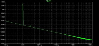
Harmonic Frequency Fourier Normalized Phase Normalized
Number [Hz] Component Component [degree] Phase [deg]
1 1.000e+03 4.189e+01 1.000e+00 -0.17? 0.00?
2 2.000e+03 6.321e-05 1.509e-06 -154.00? -153.83?
3 3.000e+03 1.081e-04 2.582e-06 99.19? 99.36?
4 4.000e+03 2.810e-05 6.709e-07 -177.44? -177.27?
5 5.000e+03 2.176e-05 5.195e-07 -135.07? -134.89?
6 6.000e+03 1.504e-05 3.590e-07 176.61? 176.78?
7 7.000e+03 1.545e-05 3.688e-07 170.02? 170.19?
8 8.000e+03 1.234e-05 2.945e-07 -178.92? -178.74?
9 9.000e+03 1.035e-05 2.471e-07 -176.88? -176.71?
Total Harmonic Distortion: 0.000317%
When bias it in class-A the higher order harmonics will be eliminated, but the total distortion figure does not change much from class-AB. 🙄
This is really a great forum for audiophiles. I have learned a lot from people in this forum. 😀
Special thanks to BV, zenelectro, and JCX. BV contributes many good improvements to this design. Zenelectro pointed a critical change to stabilize the original design. JCX also pointed some flaw in the design, which prompted me to search for better solution. I also would like to thank, greierasul, D. Self, Kastor, Bonsai, iko, bimo, and many others who contributed ideas and given good suggestions.
Hi mates,
This is to report the latest implementation results.
Some modifications have been made to the circuit in the opening post. Firstly, in the VAS, as zenelectro and Douglas Self mentioned, the compensation cap C12 is modified to across the whole Baxandall pair formed by Q14 and Q10. R36 is increased from 1150ohm to 33k, so that it supplies about 1.6 mA enough but not excessive bias current to the Q14 emitter. C2 and R7 are removed from the base circuit of Q14, since they neither help to eliminate the high frequency parasitics nor help the VAS recover better from clipping. The Q13 is also removed from the constant current source since it does not help here (maybe it does, but just does not show by Spice simulation). Secondly, two 100ohm emitter resistors are added to the LTP Q11 and Q12, also the emitter resistors of the current mirror is reduced from 690ohm to 47 ohm as suggested by BV. These changes, I hope, help to linearize the input stage and the VAS. And then, the output stage is changed to compound quasi complementary with Mosfet as output transistors. Reason for changing the output from bjt to Mosfet is that I want to use TO3 metal can transistors for good thermal stability and achieve good linearity at large load such as 2 to 4ohm, where current may > 10A. In viewing hfe-Ic curves of the popular TO3 bjt transistors, I have not found any good ones for this purposes. I happen to have some older 2SK313 metal cans, so I used them in the implementation. I am not sure if the old slow 2SK313 is the right choice for this amp, but it has a rated Idmax of 12A and small input capacitance, and it is designed for high frequency amplification as stated in the datasheet (see attached). For the two driver transistors, I actually use 2SA1930/C5171, which is more modern than the old fashioned TIPs.
Figure1.

The finished amp is shown in the above Figure1. I have measured the amp with since and sq wave, and listening-tested this amp with a +/-30V DC power supply. The frequency response roughly replicates the Spice simulation. I also have not implemented the low pass filter inductor L1 and R21. My scope can show frequency up to 100MHz. There is no resonance at any frequency up to 200KHz sq wave, higher frequency sq ware signal not tested. Sound is ok but nothing particular to mention. At least when there is no signal, the amp is deadly quiet.

The current LTspice simulation results is 0.0053% THD at 10KHz 84vpp sine wave to 8ohm load.
Harmonic Frequency Fourier Normalized Phase Normalized
Number [Hz] Component Component [degree] Phase [deg]
1 1.000e+04 4.184e+01 1.000e+00 -2.48? 0.00?
2 2.000e+04 8.562e-04 2.046e-05 85.44? 87.92?
3 3.000e+04 1.433e-03 3.425e-05 135.12? 137.61?
4 4.000e+04 5.211e-04 1.245e-05 90.62? 93.10?
5 5.000e+04 7.201e-04 1.721e-05 -28.20? -25.72?
6 6.000e+04 9.079e-04 2.170e-05 81.75? 84.23?
7 7.000e+04 3.668e-04 8.766e-06 103.40? 105.88?
8 8.000e+04 5.804e-04 1.387e-05 84.51? 86.99?
9 9.000e+04 4.048e-04 9.674e-06 69.16? 71.64?
Total Harmonic Distortion: 0.005363%

0.000298% THD at 1KHz 84vpp sine wave to 8ohm load.
Harmonic Frequency Fourier Normalized Phase Normalized
Number [Hz] Component Component [degree] Phase [deg]
1 1.000e+03 4.189e+01 1.000e+00 -0.17? 0.00?
2 2.000e+03 4.436e-05 1.059e-06 -158.28? -158.11?
3 3.000e+03 8.531e-05 2.037e-06 101.42? 101.60?
4 4.000e+03 2.388e-05 5.702e-07 160.17? 160.35?
5 5.000e+03 2.283e-05 5.450e-07 -125.70? -125.53?
6 6.000e+03 1.547e-05 3.692e-07 134.31? 134.48?
7 7.000e+03 4.073e-05 9.723e-07 110.79? 110.97?
8 8.000e+03 1.153e-05 2.753e-07 138.33? 138.51?
9 9.000e+03 5.629e-05 1.344e-06 99.13? 99.31?
Total Harmonic Distortion: 0.000298%

Harmonic Frequency Fourier Normalized Phase Normalized
Number [Hz] Component Component [degree] Phase [deg]
1 1.000e+03 4.189e+01 1.000e+00 -0.17? 0.00?
2 2.000e+03 6.321e-05 1.509e-06 -154.00? -153.83?
3 3.000e+03 1.081e-04 2.582e-06 99.19? 99.36?
4 4.000e+03 2.810e-05 6.709e-07 -177.44? -177.27?
5 5.000e+03 2.176e-05 5.195e-07 -135.07? -134.89?
6 6.000e+03 1.504e-05 3.590e-07 176.61? 176.78?
7 7.000e+03 1.545e-05 3.688e-07 170.02? 170.19?
8 8.000e+03 1.234e-05 2.945e-07 -178.92? -178.74?
9 9.000e+03 1.035e-05 2.471e-07 -176.88? -176.71?
Total Harmonic Distortion: 0.000317%
When bias it in class-A the higher order harmonics will be eliminated, but the total distortion figure does not change much from class-AB. 🙄

This is really a great forum for audiophiles. I have learned a lot from people in this forum. 😀
Special thanks to BV, zenelectro, and JCX. BV contributes many good improvements to this design. Zenelectro pointed a critical change to stabilize the original design. JCX also pointed some flaw in the design, which prompted me to search for better solution. I also would like to thank, greierasul, D. Self, Kastor, Bonsai, iko, bimo, and many others who contributed ideas and given good suggestions.
Jcx can you clarify this
...
Are you referring to something like 20 kHz = 50 uS so settling time of 1 uS is irrelevant?
Maybe it is not the setting time itself, but the mechanism, that generates the high overshoot and long setting time, matters?
If so, I will be wondering what why and how a high freq. low THD amp will be having that long setting time.
"How do you think about the below circuit? Simulation shows super low THD. Is it realistic to build such an amp?"
no, it's mandatory 🙂
Hi adason,
I have built the amp(see two levels up).Wish to have an AP to measure it.
Jazz
phase margin
Hi Bigun,
I cannot tell whether there is enough phase margin. BV's simulation shows a stable amp of this topology with 0.003%THD. In the implementation, I have made it a quasi-complementary mosfet output, and used some old verticle mosfets as the output transistor. See the post83#. I monitor the amp current and wave form, and no oscllation is found.
Jazz
how much phase margin do you have at unity open loop gain ?
Hi Bigun,
I cannot tell whether there is enough phase margin. BV's simulation shows a stable amp of this topology with 0.003%THD. In the implementation, I have made it a quasi-complementary mosfet output, and used some old verticle mosfets as the output transistor. See the post83#. I monitor the amp current and wave form, and no oscllation is found.
Jazz
you could save some time by reading a later edition of Self's Audio Power Amplifier design book, and Cordell's too
I really doubt that circuit is up to it in the real world
then there is the learning curve on physical implementation, layout, supply/gnd routing, bypassing
don't expect to get there in one try
how much phase margin do you have at unity open loop gain ?
Hi JCX,
Thank you for your good suggestions. I have been reading D. Self's "Audio Power Amplifier Design Handbook" for a few years. There are a lot of good staff to digest.
Jazz
VCE max. of BC550C is 45V and you use +-48V power supply.
Usually if you looking for low THD, you get low slew rate.
In my last design of such topology, first I looking for highest slew rate, then lowest THD20.
Hi Bimo,
In the implementation, I used BC556/546 for the input stage. In your opinion how to increase the slew rate on such a Linn topology 3 stage voltage feedback amp? I am not sure how THD at 20KHz means anything to my ears. But you are absolutely right if you mean that low THD@20K is an important parameter to look at and post a challenge for modern power amps.
Jazz
On the contrary, they will see much less than 48 volts. 😉
Vas is a baxandall pair, Cob here doesnt contribute significantly to high frequency THD.
Manso, what do you think about using the baxandall pair at the VAS? Your opinion is valued. Thank you.
Jazz
To put things in perspective here
10uA glowing through 0.1 Ohm is 1uV
1uV of 2nd harmonic on a ground return is -120 dB ref 1V signal = 1ppm (0.0001%).
10's of uA flowing through sub 1 Ohm resistances on ground tracks is a common occurence in amplifiers.
So, better to spend much effort on thinking about the practicalities of building a sub ppm amplifier - the realities are that it is extrmely difficult and its not the circuit topology thats the limiting factor in most cases, but the implementation.
Also, keep in mind you will not be able to distinguish between 0.005 and .001 distortion. A good pair of ears and some practice and you may be able to do it reliably at 0.1%.
Dont get hung up on THD.
Hi Bonsai,
You are absolutely right that it is easier in simulation than in implementation. Somebody tells me that making the +&- power tracks as close as possible is impotant in the PCB layout. However I see a lot of the amps in this forum, including some designed by Alex MM, just leave them apart, ie. one at each side of a PCB.
I believe most people do not ditinguish that small difference. Strangely I can distinguish a SennheiserHD800 from HD600 headphone just by a few seconds's listening. They both have <1% THD on paper. Do you have the same experience?
Jazz
Well, this is actually what the trade-off is about...
Open loop gain is 130 db. Closed loop gain you want to achieve would be something like 29 db. So, you have to "kill" more than 100 db with the global NFB. In such situation, almost any circuit, even with horrible open-loop linearity, will show excellent THD with the loop being closed. However, the problem is - it will tend to oscillate badly. I'm not saying it will be impossible to stabilize it, but rather difficult for sure, most likely jeopardizing some other important parameters, like slew rate and/or inter-modulation distortion (very important for sound quality!), audio bandwidth phase response, etc. So... low THD is a good thing to have, but in a proper balance with the other qualities.
Cheers,
Valery
Hi Valery,
The latest changes in simulation and implementation results are in post 83#. Your ideas are welcome.
Jazz
Last edited:
The classic flaw of this schematic and the reason it is showing such a)low
distortion and b) poor stability is simple:
The 100p Miller compensation is across only half of the Baxandall Pair, as such the B.P. essentially defeats it completely, just like it defeats the
Cob of that transistor.
Strap the 100p across both Q1 and Q12.
On the other side, no need for the 100p, it's just a current source.
If anything this baxandall pair CCS may need some taming with a base stopper on Q10.
I re ran the sim as such and the distortion is around 0.01 at 28V peak / 8
ohm.
Oh well no free lunch 🙂
Z
Hi Zenelectro,
Thank you very much for pointing out the flaw in stability. I simulated a classical Naim NAP140 amp, which is what this amp is based on. The Naim NAP140 with minor modifications to componnent selection and values, can achieve 0.01% THD. This low distortion amp, with the improved input and VAS stages, should be much better that a Naim.
Jazz
Hi Bimo,
In the implementation, I used BC556/546 for the input stage. In your opinion how to increase the slew rate on such a Linn topology 3 stage voltage feedback amp? I am not sure how THD at 20KHz means anything to my ears. But you are absolutely right if you mean that low THD@20K is an important parameter to look at and post a challenge for modern power amps.
Jazz
To increase the slew rate, use high current tail for the LTP, but must considered with dissipation of the LTP transistor. Of course the noise will be increase too, but it can be accepted on an power amplifier.
You can play with R degen at LTP. High R degen will increase slew rate, but lowered the open loop gain and increase noise too.
For simple Lin topology, I like use C miller and C lead for compensation (see AKSA 55). It will increase the slew rate.
For complex Lin topology I will use TMC for compensation. It give lower THD at high frequency.
I still do not understand why high slew rate sound good to my ear. I found not all high slew rate design is also give lower intermodulation (IM) distortion. I ask Bob Cordell to discuss how to lowered IM distortion on the his new book.
You should try your self to compare high slew rate amp and low slew rate amp.
Hi Zenelectro,
Thank you very much for pointing out the flaw in stability. I simulated a classical Naim NAP140 amp, which is what this amp is based on. The Naim NAP140 with minor modifications to componnent selection and values, can achieve 0.01% THD. This low distortion amp, with the improved input and VAS stages, should be much better that a Naim.
Jazz
No worries.
It's good to see you are enjoying the learning experience of developing this
circuit, that's a big part of what this forum (should be) is about.
WRT Baxandall pair, they are generally used to negate a reactive capacitance
and in particular a voltage modulated capacitance as is seen across most
semiconductors. For example, in a CCS this Cob capacitance may manifest
as a much reduced OP impedance at high frequencies then implementing a
Baxandall pair in the CCS output will keep the impedance much flatter as
frequency rises.
In the case of the voltage stage in an amplifier you have too look at -all- the
capacitances that the stage sees. So in an amplifier that has a two stage BJT
OP, the driver transistors will be solid medium power devices, as such they
will have significant Cob and this will dominate what the voltage stage has
to drive.
I haven't followed this thread but I see your latest amplifier uses BJT driven
MosFET OP stage which I like a lot. Intuitively a lot of people think this
approach is somewhat back to front but it has some definite advantages WRT
the non linear load of the MOSFET capacitances.
In your case I would spend some time experimenting on the OP stage with
some very fast BJT's to drive the MOSFETs. They don't necessarily have to
be 1A devices. Look for very low and linear Cob and say a few hundred mA
drive capability.
There will be 2 main sources of distortion in this voltage stage, a) The non
linear Cob of the driver transistors, b) The non linear effects of C12
compensation capacitor. As you load the OP stage with say 4 ohms, since
the MOSFETs have fairly low gm compared to a BJT OP, this stage will be
swinging in a non linear fashion to keep the OP swing linear. As frequency
rises this non linear swing basically makes C12 look like a non linear
load and there's your rising distortion with rising frequency.
Same goes with xover distortion.
Your simulated results show this quite clearly.
Personally I try to achieve simulated distortion results below 0.001% at
20kHz into 2 ohms with around 30 to 40V peak swing out of a simple
circuit with good phase margin.
If the design can achieve this it will have a pretty good chance of measuring
very well in real life given a lot of attention is paid to layout etc.
cheers
T
Slew Rate
Yes. It is stated clearly in Self's book Audio Power Amp Design Notes that increasing the LTP current will make the S/R higher. But to maintain something else(transconductance, if I remember correctly), it is also needed to increase the degeneration resistance. He suggests to use 3mA for each transistor of the LTP.
Thanks for referring me to the AKSA55. I have found Greg Erskine's thread. Very good stuff to read. The circuit diagram looks not complete, but enough information to see the topology. I also find a version by Rod Elliot(http://www.radioland.net.ua/sxemaid-146.html), which uses no bootstrapping at the input. Do you think it is the bootstrapping at the input and/or VAS that does the magic?
IMHO, high slew rate amps makes high frequency hamonics more apparent. But if the amp has high odd order hamonics to ultrasonic, the sound may be horrible. I think this is one of the things that distinguishs most tube and solid state.
Jazz
To increase the slew rate, use high current tail for the LTP, but must considered with dissipation of the LTP transistor. Of course the noise will be increase too, but it can be accepted on an power amplifier.
You can play with R degen at LTP. High R degen will increase slew rate, but lowered the open loop gain and increase noise too.
For simple Lin topology, I like use C miller and C lead for compensation (see AKSA 55). It will increase the slew rate.
For complex Lin topology I will use TMC for compensation. It give lower THD at high frequency.
I still do not understand why high slew rate sound good to my ear. I found not all high slew rate design is also give lower intermodulation (IM) distortion. I ask Bob Cordell to discuss how to lowered IM distortion on the his new book.
You should try your self to compare high slew rate amp and low slew rate amp.
Yes. It is stated clearly in Self's book Audio Power Amp Design Notes that increasing the LTP current will make the S/R higher. But to maintain something else(transconductance, if I remember correctly), it is also needed to increase the degeneration resistance. He suggests to use 3mA for each transistor of the LTP.
Thanks for referring me to the AKSA55. I have found Greg Erskine's thread. Very good stuff to read. The circuit diagram looks not complete, but enough information to see the topology. I also find a version by Rod Elliot(http://www.radioland.net.ua/sxemaid-146.html), which uses no bootstrapping at the input. Do you think it is the bootstrapping at the input and/or VAS that does the magic?
IMHO, high slew rate amps makes high frequency hamonics more apparent. But if the amp has high odd order hamonics to ultrasonic, the sound may be horrible. I think this is one of the things that distinguishs most tube and solid state.
Jazz
Last edited:
No worries.
...
T
Really appreciate that you take time and wrote so much valueble information.😛
Now I have heard two different sayings wrt the output impedance of the Baxandall pair acting as CCS. If the Baxandall pair really helps to flat the impedance to higher frequencies, should that manifest in the simulation? I am wondering why it did not show any benefit in my simulation of THD@10KHz, which is almost the same using normal or Baxandall pair CCS(with or without Q13 in the openning post)😕. But I think the VAS in this circuit is basicly another Baxandall pair in complementary to the VAS CCS, which has distinuished effects on minimise the load to the front and output impedance, and also shows benefits in THD simulation.
The 2SK313(I use in my implementation) input capacitance is 1500pF(Vds10V, Vgs 0V, f=1MHz), which is slightly higher than the IRFP240's 1300pF(Vds25V, Vgs 0V, f=1MHz), but the output capacitance is 330pF, and the reverse transfer capacitance is 35pF, both lower than IRFP240's 400pF and 130pF. The Rds max for 2SK313 is 0.9ohm vs. IRFP240's 0.18ohm. Any comments on using 2SK313 vs. using IFRP240 for the op?
Is it realistic to minimise the non-linear effect of the output transistor input capacitance by using higher drive current and lower resistance of the driver emitter resistor R19 and R22, and of the base stopper? For example, if I reduce the resistance of R19 and R22 to 33ohm, I will need to increase the drive bias current from 40mA to 120mA. The 2SA1930/C5171 have Pc 20W, fT200MHz, output capacitance 26pF and 16pF respectively. Do you think they are good enough to be drivers here? If another pre-driver stage is added to the output, it could make the VAS load even lower. However, it seems that nobody uses tripples for mosfet output. Maybe they think it unnecessary and too hard to get it stable.
Jazz
Hi Valery,
The latest changes in simulation and implementation results are in post 83#. Your ideas are welcome.
Jazz
Hi Jazz,
Sorry if I have missed something - 2 questions about topologies I would consider as an alternative to see if they bring some benefits:
1) Same voltage amplification section, but with complementary output pairs;
2) Same quasi-complementary OPS, but balanced VAS, so that both "shoulders" are fully identical (if you need more details on this one, I can draw a sketch) - it normally gives a good phase response, requiring lighter compensation.
I mean, did you consider these options at some point?
What advantages/disadvantages do you see (if any)?
Thank you,
Valery
Have you built the amp and measured the THD yet?
I don't mean to be a party pooper, but in my experience, the simulators are often way over-optimistic on the THD. I suspect the various device models are linearized to fit the curve trace data while still being "friendly" to the simulator (i.e. allow for convergence and for the simulation to run in a reasonable amount of time).
Also note that the circuit layout plays a large role in a precision circuit. You may be able to take a few layout pointers from my LM3886 PCB vs P2P (with data) thread. I found that the THD, in particular, beyond 1 kHz was highly layout dependent. With a discrete amp, you will have more layout to worry about. In particular, the nodes around your input stage and biasing circuit will need to be carefully thought out.
The name of the game is inductance. Minimize it!
It looks like you have a pretty solid circuit in the simulator. I'm curious to see how well it correlates with reality. I did see the implementation in Post #83, but there was no measured data. Only simulation data. Am I missing something?
~Tom
Hi Jazz,
...
I mean, did you consider these options at some point?
What advantages/disadvantages do you see (if any)?
Thank you,
Valery
Hi Valery,
I have considered complementary since the start of this design. It, in theory, should be easier to achieve lower distortion. I have 4 pairs of Sanken 2SA1216/C2922 at my hand. However the measured HFE(10mA Ib) differs a lot. For example, one C2922 measured 45, the other 58. To make the amp practical, I choose to use most common vertical mosfet for the output. Balanced VAS is also a good idea in theory. It face the same difficulty of matching parts.
IMHO, the good thing with Linn topology is that you do not need to spend big effort on matching parts, and it is very tolerant to parts parameter deviation. I could be wrong on this, but I hope not, because it is one of the the things that triggerred me to making this design.
Jazz
Thanks for referring me to the AKSA55. I have found Greg Erskine's thread. Very good stuff to read. The circuit diagram looks not complete, but enough information to see the topology. I also find a version by Rod Elliot(55?? (????????????? 75??) ????????? ???????? - ????? - Radioland), which uses no bootstrapping at the input. Do you think it is the bootstrapping at the input and/or VAS that does the magic?
IMHO, high slew rate amps makes high frequency hamonics more apparent. But if the amp has high odd order hamonics to ultrasonic, the sound may be horrible. I think this is one of the things that distinguishs most tube and solid state.
Jazz
The magic of AKSA55 is the THD profile is like tube and the slew rate is high.
These are the result of simulation of my blameless amplifier:
Phase Margin 66. Gain Margin 8.
THD at 71W/8Ohm, 20kHz -> 0.000287%
THD at 142W/4Ohm, 20kHz -> 0.000537%
PSRR at 100Hz -> 118 dB
Slew Rate 90V/µS
I use +-44V DC power supply.
And the sound is really good 😉
- Status
- Not open for further replies.
- Home
- Amplifiers
- Solid State
- THD=0.000048% Voltage Feedback Amp