... slew rate limiting ... will manifest itself in the VBE of the output emitter follower Q503 ...
Duh, now I realize that in this topology, it will be a LOT easier just to monitor the emitter currents of the output stage pullup and pulldown, Q503 and Q504. If Q503's current ever falls below 10% of Q504's current, the circuit is obviously and unarguably slew rate limiting, HARD. Simple to plot and easy to judge by eyeball. Run it at 50 kHz with carefully chosen max-amplitude, per Bob Cordell.
Some of us ultra-nosebleed-feedback type people, prefer to build circuits that are not slew rate limited when reproducing 200 kHz, max-output-amplitude sinewaves. A factor of four more difficult than Bob Cordell recommends in his introductory textbook. "If some is good then more is better" -- US Army field guide to demolition explosives.
Example math: ±29V rails preamp is able to create ±20V peak-to-peak sine waves at its output. Max required slew rate at 50 kHz = dV/dt = 20 * 2 * pi * 5E4 = 6.3 volts/microsecond. So build your circuit to slew at 1.5X or 2.0X this requirement: namely 9.4 V/us or 12.6 V/us. Unless you're a nosebleeder; in that case, multiply by 4X.
Member
Joined 2009
Paid Member
If Q503's current ever falls below 10% of Q504's current, the circuit is obviously and unarguably slew rate limiting, HARD. Simple to plot and easy to judge by eyeball. Run it at 50 kHz with carefully chosen max-amplitude, per Bob Cordell.
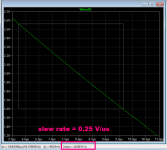
At 50kHz with +/- 1.4V at the output we 'pass' this test. I can see that it would look less favourable at much higher swings. Is it a simple case of increasing the idle current through the output ?
Nigel - yes, I believe that is the reason for favouring passive at h.f.
When you try it you will discover the answer is no. James E. Solomon's landmark paper with the oft-cited slew rate formulae, is no help to you, because you don't have a long tailed pair with current source. You'll have to derive your own formulae to calculate the slew rate, then identify the mechanism which limits it. I'm willing to bet a case of Guinness it won't turn out to be the output current sink.
Member
Joined 2009
Paid Member
I don't have the interest to derive an empirical analysis! I am even wondering if there is anything to be concerned about regarding normal use. The slew rate looks OK unless there is a need to design for parasitic ultra-sonics or heroic recovery from large 'clicks & pops'. Increasing the feedback network impedance is one way to provide more slew-rate headroom at the expense of higher noise (which is likely dominated by the vinyl surface anyway). However, a smaller capacitor in the feedback shunt position has some benefits and I could provide footprint for two choices for flexibility. I found a discussion on the Graham Slee forum where the 200kHz number is bandied about. Yikes.
About that Guinness - I assume some improvement in slew rate would be achived from higher idle current because the increase in gm will reduced Zout.
About that Guinness - I assume some improvement in slew rate would be achived from higher idle current because the increase in gm will reduced Zout.
Last edited:
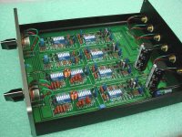
90mm x 31mm PCB
Turn-on delay adjustable via 20-turn trimpot #1, from 2 seconds to 40 seconds
Turn-off delay adjustable via 20-turn trimpot #2, from 200 milliseconds to 4 seconds
Turn-on delay adjustable via 20-turn trimpot #1, from 2 seconds to 40 seconds
Turn-off delay adjustable via 20-turn trimpot #2, from 200 milliseconds to 4 seconds
Slew rate = 0.25 volts per microsecond (!)
I think you've still got quite a ways to go yet.
For reference, the uA741 opamp chip's slew rate was 0.5 V/usec.
Part of your problem is the unfortunate choice of a ridiculously low bandwidth opamp in the inverse RIAA network. I recommend replacing it with either a 50 MHz opamp or a source follower running at healthy bias current.
Attachments
Member
Joined 2009
Paid Member
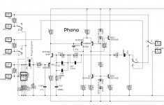
For a simple analysis we don't need to include the inverse RIAA network at all. I can try that. But the basic phono amp - if the slew rate is traditionally limited by Cdom then we can calculate it using i/Cd. With, say, 300uA flowing through the input pair the max drive current into Cdom can be 300uA which gives a slew-rate of over 6V/us. I think I showed 47p in my diagrams, the original NAD actually used only 10p so I've made things worse with this part labeling and it's more like 30V/us.
Member
Joined 2009
Paid Member
Board#3
Board#3 is the last board, after that I'm out of space in the chassis. For this board I'm considering a cross-over so that I can make some use of the various amplifiers I have to bi-amp my speakers. The original idea I had was to make a pair of FAST speakers (this acronym escapes me, but it's a full range driver with supporting woofer) where the XO will be around 300Hz. With some flexibility I would be interested to try bi-amping my current floor-standing speakers which are the more traditional mid-woof and tweeter with a 2kHz XO. Nelson Pass 'B4' active XO is a potential role-model for this idea. Passive switch-selectable filters with simple buffers.
So at the end of it the box will have input & phono (#1), tone & line-out (#2), line-level cross-over (#3).
Attachments
Last edited:
For a simple analysis we don't need to include the inverse RIAA network at all. I can try that. But the basic phono amp - if the slew rate is traditionally limited by Cdom then we can calculate it using i/Cd. With, say, 300uA flowing through the input pair the max drive current into Cdom can be 300uA which gives a slew-rate of over 6V/us. I think I showed 47p in my diagrams, the original NAD actually used only 10p so I've made things worse with this part labeling and it's more like 30V/us.
Think back to what the circuit was like before you increased that Cdom and what prompted you - for instance was it before or after you decimated the impedance of your RIAA feedback network in comparison the NAD equivalent.
Your increase R31 from 56k to 91k is strange when this element is to supply base current to your addition of Q1.
Member
Joined 2009
Paid Member
I believe the Cdom was a typo, not an intentional increase. I have actually decreased the closed-loop gain from the NAD so no reason to increase Cdom for the sake of stability. Mind you, I also added an output buffer, more phase shift inside the feedback loop.
I believe R31 was increased to maintain the same current level, roughly, after I increased the -ve rail. I'll have to check again as I don't have access to the files from where I'm sitting at present.
I believe R31 was increased to maintain the same current level, roughly, after I increased the -ve rail. I'll have to check again as I don't have access to the files from where I'm sitting at present.
Last edited:
I think you'll find that the base and emitter of output pullup Q503, move in phase with each other. They either both rise or they both fall.
During the worst-case, ugliest slew event, they both fall. The collectors of both current sink transistors (Q410 & Q504) both fall. Thus the collector-base capacitances of Q410+Q504, tug down the base node when the collectors fall. And boy howdy is this just what you DO NOT WANT! Exactly when you want the current sinks to really sink some current, their VBE is reduced by capacitive coupling. In one simulation I ran, the "constant current source" transistors' collector current, fell by a factor of 3X during slewing. Ouch!
Douglas Self's APAD6 discusses this in Chapter 15, under the heading "Slewing Limitations In Real Life". Regrettably, Self's suggested fixup requires a change to your PCB layout. Self shows his repair method in Fig 15.7, but it is rather invasive surgery, replacing (2 diodes) with (1 BJT + 1 resistor + 1 capacitor). Other fixes may require less radical surgery. You can try out various ideas in LTSPICE as they pop into your head, to determine which is the least horrifying to your own personal sensibilities.
Jim Solomon's equation "SlewRate = dV/dt = Ibias/Cdom" is completely inapplicable here, because the Rush Cascode does not have a constant tail current you can call "Ibias". During slewing, the current available to charge or discharge the "compensation capacitor" is wildly non-constant. Furthermore, because there is no current mirror, slew rate is different for the rising edge than for the falling edge.
If you decide to eliminate the inverse-RIAA network at the input, be sure to apply input signals with extremely fast rising edges and falling edges. The RIAA preamp includes two poles and a zero, so it acts as lowpass filter. If you want to see a fast (slew-limited) edge on the output, apply an extremely fast edge at the input.
Attachments
Member
Joined 2009
Paid Member
Self shows his repair method in Fig 15.7, but it is rather invasive surgery, replacing (2 diodes) with (1 BJT + 1 resistor + 1 capacitor). Other fixes may require less radical surgery. You can try out various ideas in LTSPICE as they pop into your head, to determine which is the least horrifying to your own personal sensibilities.
I remember reading about this one, but if I remember, it's a form of positive feedback from the collector of the current source to the base of the transistor controlling said current source - which requires some care to avoid creating a bigger problem than you are trying to solve.
Let me try a different way of looking at this to see if it makes more sense to me.
The concern is whether the output stage can drive the feedback network at high frequencies because this is where the series impedance of the feedback network falls off rapidly. Worse case is that the output stage has to source the current to charge/discharge the feedback shunt capacitor through the feedback shunt resistor.
The voltage swing across the feedback shunt network, i.e. at the feedback node, should be the same as the input signal if the amplifier is not distorting.
A nominal MM cartridge output is rated at 5mV (1kHz) and rises with frequency so at 20kHz it would be ten times higher. And allowing for up to 20dB peaks on top of that would be another factor of ten. That’s a huge 500mV input signal, with peak of sqrt(2) x 500 = 700mV.
If the feedback node has to match this, the output stage has to provide peak current of 2 x Pi x f x Vp x Cs. For a 470uF shunt capacitor thats 41mA. Yikes. The original NAD design value of 47uF with a higher impedance feedback network looks far more reasonable.
Last edited:
Slewing happens when a transistor turns completely off.
In the Solomon / conventional LTP circuit, one of the two transistors in the LTP turns completely off, and 100% of the LTP tail current is steered (via the current mirror) into the compensation capacitor. When a constant current charges a fixed capacitor, the slew rate dV/dt is equal to (Itail/C) -- the Solomon slew rate equation.
In this Rush Cascode circuit, the common base PNP transistor Q408 turns completely off during worst case slewing (downward), because its base is fixed at (2 diodes below +Rail) but its emitter gets sharply yanked downward by Q406. Result: Emitter-to-Base voltage is reduced and Q408 turns completely off. The collector of Q408 falls like a rock, which immediately cuts off the output pullup Q503. Two of the seven transistors in the circuit, are completely cut off. Ouch! Not a prescription for distortion free amplification.
You can hunt through all those previously posted variants of Rush Cascode input stage, RIAA preamps, to discover how they deal with slewing. Maybe there are several not-so-obvious tweaks to circuit topology or to component values, which cumulatively produce a greatly improved slew rate. Or maybe this circuit is forever doomed to have worse slew rate than the uA741 opamp. I myself have neither built nor measured a Rush Cascode RIAA amp, so I can't tell you what its real-life, real-world slew rate actually is.
Maybe someone in this thread can measure the slew rate of one of those NADs / other Rush Cascode RIAA products. Or maybe someone has a specification sheet for one of them, which quotes a slew rate for the phono stage. Line stage slew rate is likely to be vastly larger.
Last edited:
Member
Joined 2009
Paid Member
Now you've lost me. I have never seen 'slewing' limited to use when devices are turned-off. I've seen it used only to describe the rate of change of an output voltage. Anyhow, under what conditions do you see Q408 being driven hard enough to turn off - ? At this extreme we're talking about an input signal so large it causes the input pair to exceed their Class A operating range. That requires an input level beyond the design remit of a phono amp doesn't it ?
Member
Joined 2009
Paid Member
Are we talking about the low or high impedance feedback network? I can see the amp fall-over badly if driven too hard with the low impedance fdbk but this goes away when I return to the original high impedance network.
Are we talking about the low or high impedance feedback network? I can see the amp fall-over badly if driven too hard with the low impedance fdbk but this goes away when I return to the original high impedance network.
Q408 (NAD) is equivalent to your Q13.
Member
Joined 2009
Paid Member
I've been messing around with part numbers.
I can see that when the output stage can't drive the feedback network then the error amplifier isn't getting what it needs, it 'sees' a much larger error and tries to correct - and runs out of range. The downside of the high impedance network is, as I understand, higher noise levels into the error amplifier. As far as I know, all phono amps have to make a tradeoff between slew rate and noise ?
I can see that when the output stage can't drive the feedback network then the error amplifier isn't getting what it needs, it 'sees' a much larger error and tries to correct - and runs out of range. The downside of the high impedance network is, as I understand, higher noise levels into the error amplifier. As far as I know, all phono amps have to make a tradeoff between slew rate and noise ?
It sounds like you now have a version which exhibits no slew rate anomalies at all. Congratulations!
I gently suggest you simulate it with input driven by a tall enough, fast enough sinewave to put the amplifier into obvious slewing, and then measure the slew rate itself: dV/dt. Who knows, you might have accidentally created a circuit that slews at 25 V/usec or even faster. Which would satisfy and delight even the ultra-feedback-nosebleeders like me, who insist upon no-slew, full power bandwidth > 200 kHz.
When sinewaves go in and triangle waves come out, yer slewing. Easy. Once you've got the thing to slew, go digging internally and you'll find at least one transistor is cut off. Honest.
- Status
- Not open for further replies.
- Home
- Source & Line
- Analog Line Level
- TGMC - a modular control pre-amplifier