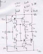
This picture explains better my approach for the bias string and thermal compensation of the OPS based on LTspice simulations. Convenient for construction too.
Damir
I suggested at the time doing a sim with a real speaker load i.e. change the angle of current to voltage. The fortuitous cancellation tends to go away. I will not participate in another Krill thread.
Member
Joined 2009
Paid Member
I've not tried simulating real speakers - would be willing to try if anybody has a favourite equivalent circuit. Anyhow, I'm planning to bias this up to around 26mV across the Re resistors, just like every other Class AB I've built before - it's just a Diamond Buffer output stage afterall. Maybe that was missed previously.
Where I am more concerned about 'fortuitous cancellation' is in the voltage gain stage. Simulations into resistive loads suggest this error take off approach from Mr. Kulish should be cleaner than a simple Darlington.
Where I am more concerned about 'fortuitous cancellation' is in the voltage gain stage. Simulations into resistive loads suggest this error take off approach from Mr. Kulish should be cleaner than a simple Darlington.
I didn't see this thread, but I'll add my 2 cents. The simulation models don't include quasi-saturation. Without it you may not see what is actually happening when the switching system works. Here are some models I've made or modified which have quasi-saturation.
Code:
.model BC337-40_kq NPN(IS=7.809E-14 Ibc=100f NF=0.9916 ISE=15f NE=1.4 Nk=0.55 BF=436.8 IKF=1.15 VAF=125 NR=0.991 ISC=6.66E-14 NC=1.2 BR=44.14 IKR=0.09 VAR=14 Rb=17.4 Kf=30f IRB=2.00E-04 RBM=8 RE=0.12 RC=0.05 Rco=3 XTB=0 EG=1.11 XTI=3 CJE=80p VJE=0.6657 MJE=0.3596 TF=620p XTF=1.5 VTF=2 ITF=0.5 PTF=88 CJC=1.306E-11 VJC=0.3647 MJC=0.3658 XCJC=0.455 TR=2.50E-08 CJS=0 VJS=0.75 MJS=0.333 FC=0.843 Vo=500 Gamma=4n Qco=8n Vceo=45 Icrating=800m mfg=OnSemi)
.model BC327-40_kq PNP(IS=2.077E-13 Ibc=230f NF=1.005 ISE=1.4f NE=1.3 NK=0.5 BF=475 IKF=.65 VAF=35 NR=1.002 ISC=2.963E-13 NC=1.25 BR=20.92 IKR=0.104 VAR=10 RB=17.4  Kf=240F IRB=1.00E-05 RBM=5.3 RE=0.14 RC=0.32 Rco=3.75 XTB=0 EG=1.11 XTI=3 CJE=115p VJE=0.9296 MJE=0.456 TF=500p XTF=3.25 VTF=2.5 ITF=0.79 PTF=80 CJC=2.675E-11 VJC=0.8956 MJC=0.4638 XCJC=0.459 TR=3.50E-08 CJS=0 VJS=0.75 MJS=0.333 FC=0.935 Vo=500 Gamma=10n Qco=8n Vceo=45 Icrating=800m mfg=OnSemi)
.MODEL 2SC1845E_kq npn IS=1.075431E-13 BF=600.7 NF=1 BR=13.565 NR=1
+ ISE=1.98107E-13 NE=2 ISC=1.8378E-11 NC=1.5 VAF=200 VAR=20.6691
+ IKF=55m Nk=0.66 IKR=0.0190546 RB=157 RBM=12.092 IRB=1.258925E-6 RE=1.5
+ RC=1 CJE=18p VJE=0.7300286 MJE=0.3619943 FC=0.5 CJC=4.525739E-12
+ VJC=0.5 MJC=0.3659045 XTB=1.7281 EG=1.1809 XTI=3 Tf=420p Itf=20m
+ Xtf=1 Rco=250 gamma=2u Vo=500 Vceo=120 Icrating=50m mfg=NEC
.model KSC1845F_kq ako:2SC1845E_kq NPN Vceo=120 Icrating=50m mfg=Fairchild
+ Bf=355 Ikf=300m Vaf=400 Ise=1000f Ibc=600f
+ Rco=150 Gamma=10u Vo=9 Isc=22f
.MODEL 2SA992F_kq pnp (IS=5.7544E-14 BF=348.1 NF=1 BR=3.62 NR=0.95
+ ISE=5.7544E-15 NE=1.5 ISC=1.8378E-14 NC=1 VAF=50 VAR=16.68 IKF=0.298
+ IKR=0.0525 RB=140 RBM=16.084 IRB=1.4125E-3 RE=0.3 RC=100m CJE=13p
+ VJE=0.855 MJE=0.4104 FC=0.5 CJC=8.9251E-12 VJC=0.5 MJC=0.3497 CJS=0
+ VJS=0.8 MJS=0.33 XTB=1.2849 EG=1.1603 XTI=3 XCJC=0.3062 Tf=420p Itf=5
+ Xtf=.5 Vceo=120 Icrating=50m mfg=NEC Rco=100 gamma=200n Vo=500)
.model KSA992F_kq ako:2SA992F_kq PNP Vceo=120 Icrating=50m mfg=Fairchild
+ Bf=404 Vaf=110 Ikf=150m Ise=15f Isc=0.0010f
+ Rco=70 Rc=0 Gamma=1500n Vo=100 Ibc=45f Is=75f
.MODEL 2SC4883A_kq npn (Bf=140 Ikf=100 Is=600f Vaf=500
+ Rb=1.7 Re=105m RC=0 Rco=6 Ibc=150f Vo=30 Gamma=250n
+ Cje=1.2n Cjc=72p Tf=875p Vtf=1.2 Itf=1 Qco=8p
+ Nk=1.2 Br=2 Var=22.9 Ikr=36 TR=85n
+ Xtb=0.34 Xtf=1.36
+ Vceo=180 Icrating=2A mfg=Sanken)
.MODEL 2SA1859A_kq pnp (Bf=162 IKF=10 Is=500f Vaf=350
+ Rb=0 Re=0 Rc=90m Rco=3.25 Ibc=150f Vo=120 Gamma=22n
+ Cje=1.5n Cjc=72p Tf=1.9n Vtf=1.9 Itf=1 Qco=8p
+ Br=2 Ikr=10 Var=23 Tr=188.8n
+ Xtb=0.138 Xtf=5
+ Vceo=180 Icrating=2A mfg=Sanken)
***************************************************************************
*                                                                         *
*  2SC5171 model created by Harry Dymond. May be freely distributed with  *
*  the proviso that this header comment is included in its entirety. The  *
*  model is based on datasheet and custom measurements available at:      *
*  [url]https://dl.dropbox.com/s/v95mdjwit237sl5/transistor%20models.zip?dl=1[/url]  *
*                                                                         *
*  Please note that hFE and fT are not accurately modelled at high        *
*  current, or, in the case of fT, at low voltage. This is in order to    *
*  accurately model the transistor at low currents.                       *
*                                                                         *
*  The model has not been tested at any temperature other than 25 C       *
*                                                                         *
*  If you feel you can improve the model you are of course welcome to do  *
*  so but if you do, please let me know!                                  *
*                                                                         *
*  harry(dot)dymond(at)bristol(dot)ac(dot)uk                              *
*                                                                         *
***************************************************************************
.MODEL 2SC5171_Dkq NPN(
+IS=549.422e-15 NF=1.017914574 RB=9.805 RBM=0.1 IRB=10 VAF=250
+BF=198 NE=2.0 ISE=1e-16 IKF=1.5
+TF=700e-12 VTF=5 FC=0.5 XTF=500 ITF=20
+CJE=750e-12 MJE=0.332617 VJE=.378977
+CJC=56.636e-12 MJC=0.466097542 VJC=0.577374486
+TNOM=25 Rco=17 Gamma=6.4u Vo=1k Vceo=180 Icrating=2 mfg=Toshiba)
***************************************************************************
*                                                                         *
*  2SA1930 model created by Harry Dymond. May be freely distributed with  *
*  the proviso that this header comment is included in its entirety. The  *
*  model is based on datasheet and custom measurements available at:      *
*  [url]https://dl.dropbox.com/s/v95mdjwit237sl5/transistor%20models.zip?dl=1[/url]  *
*                                                                         *
*  Please note that hFE is not accurately modelled at high current, and   *
*  fT is not accurately modelled at low voltage. This is in order to      *
*  accurately model hFE at lower current and fT at higher voltages.       *
*                                                                         *
*  The model has not been tested at any temperature other than 25 C       *
*                                                                         *
*  If you feel you can improve the model you are of course welcome to do  *
*  so but if you do, please let me know!                                  *
*                                                                         *
*  harry(dot)dymond(at)bristol(dot)ac(dot)uk                              *
*                                                                         *
***************************************************************************
.MODEL 2SA1930_Dkq PNP(
+IS=1.573e-12 NF=1.04 RB=20 RBM=0.1 IRB=10 VAF=83
+BF=250 NE=2.154 ISE=1e-15 IKF=7 NK=0.85
+BR=4 IKR=1.05 VAR=8.3
+TF=455e-12 VTF=2.2 FC=0.5 XTF=5500 ITF=40
+CJE=640e-12 MJE=0.52939885 VJE=0.814106
+CJC=112.474e-12 MJC=0.535605 VJC=0.805555
+TNOM=25 Rco=7.3 Gamma=330n Vo=1k Vceo=180 Icrating=2 mfg=Toshiba)I will not participate in another Krill thread.
Good news..... but you just did... 🙂
cheers
Terry
Member
Joined 2009
Paid Member
Andrea Ciuffoli
Did anybody try some of the ideas from Andrea regarding this Diamond Buffer style of output:
Andrea Ciuffoli - Home Page 5 - DOCUMENTATION
Did anybody try some of the ideas from Andrea regarding this Diamond Buffer style of output:
Andrea Ciuffoli - Home Page 5 - DOCUMENTATION
Attachments
Did anybody try some of the ideas from Andrea regarding this Diamond Buffer style of output:
Andrea Ciuffoli - Home Page 5 - DOCUMENTATION
Hi Bigun!
did you analyse it? could you share your findings?
Yes, tried it on a 100W PP amp several years ago. Works very well but dimensioning the current mirrors is fiddly. Advantage is flexibility with any load.
HD
HD
Member
Joined 2009
Paid Member
I played with the ideas from Andrea only in Spice and decided it was more trouble than it's worth because I wanted to design something in Spice without doing a lot of bench testing first. This idea looks good but I thought it needed some bench testing before I'd be willing to incorporate it. And it wasn't something I thought Hugh would disclose given his product is still active. So I have kept to the simpler output structure.
As it happens, I did have a set of TGM11 PCB's fabricated but as yet no time to populate and play with them.
As it happens, I did have a set of TGM11 PCB's fabricated but as yet no time to populate and play with them.
I played with the ideas from Andrea only in Spice and decided it was more trouble than it's worth because I wanted to design something in Spice without doing a lot of bench testing first. This idea looks good but I thought it needed some bench testing before I'd be willing to incorporate it. And it wasn't something I thought Hugh would disclose given his product is still active. So I have kept to the simpler output structure.
As it happens, I did have a set of TGM11 PCB's fabricated but as yet no time to populate and play with them.
I gave up on simulations, just cannot set the parameters to simulate it right, would you drop small advice?
Attachments
Member
Joined 2009
Paid Member
I'll have a quick look when I'm back at my usual computer. If it's just a simple power buffer than it should be simple to 'fix', but if it's the more complex design that Hugh implemented I should say that this isn't something I got working to my satisfaction.
Member
Joined 2009
Paid Member
I don't want to mess around with the spice file this evening.
However, Hugh has kindly offered to make some information about his amplifier available so you have a solid place to start from. You are seeing it here for the first time !
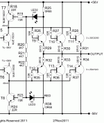
Here, I've attached a drawing of the output stage (copyright Aspen Amplifiers, all rights reserved) and a picture of a finished amplifier to drool over !
For the front end voltage amplifier feel free to use one of your favourites. For my TGM11 I'm using a simple two-transistor voltage amp.
However, Hugh has kindly offered to make some information about his amplifier available so you have a solid place to start from. You are seeing it here for the first time !
Here, I've attached a drawing of the output stage (copyright Aspen Amplifiers, all rights reserved) and a picture of a finished amplifier to drool over !
For the front end voltage amplifier feel free to use one of your favourites. For my TGM11 I'm using a simple two-transistor voltage amp.
Attachments

Thank you Gareth for teasing, I guess that this type of output was not so extraordinary to use in your amps?
Yes, tried it on a 100W PP amp several years ago. Works very well but dimensioning the current mirrors is fiddly. Advantage is flexibility with any load.
HD
Hi Hugh!
would you drop your solution for make this idea working?
with the values like attached on the scan it is not working properly...
Member
Joined 2009
Paid Member
Thank you Gareth for teasing, I guess that this type of output was not so extraordinary to use in your amps?
I didn't understand it well enough, nor could I get a satisfactory simulation running and didn't want to bench test it. So I didn't adopt it. I did include the basic buffer - you can see it somewhere earlier in this thread if you scroll back up.
I don't want to mess around with the spice file this evening.
However, Hugh has kindly offered to make some information about his amplifier available so you have a solid place to start from. You are seeing it here for the first time !
Here, I've attached a drawing of the output stage (copyright Aspen Amplifiers, all rights reserved) and a picture of a finished amplifier to drool over !
For the front end voltage amplifier feel free to use one of your favourites. For my TGM11 I'm using a simple two-transistor voltage amp.
Sensing resistors R25/38 are for modulating ops bias, but there is a positive feedbac if I see well? Raising current trough ops bjts is raising reference voltage for the ccs, so ccs is delivering current peaks on demand?
Clever idea to avoid a high biasing of T5 / T6, yet enabling them to deliver the necessary drive current for the output transistors. It also allows to dispense with a triple output stage and it's stability issues.Sensing resistors R25/38 are for modulating ops bias, but there is a positive feedbac if I see well? Raising current trough ops bjts is raising reference voltage for the ccs, so ccs is delivering current peaks on demand?
(Btw I thought Hugh is avoiding CCS's for acoustic reasons?)
[…]For my TGM11 I'm using a simple two-transistor voltage amp.
Interesting that you get enough linearity out of it to use it open loop. Must try this too one day….
Member
Joined 2009
Paid Member
- Home
- Amplifiers
- Solid State
- TGM11 - no GNFB - inspired by Steven Dunlap 'KRILL'