bootstrap cap...
Sorry, because of my poor English I didn't get the idea of eliminating the bootstrap capacitor - sounds good 😉
By the way, I've removed and shorted the electrolyte in feedback loop. The offset voltage remained around 2 mV for one channel, and 7 mV for the other.
Sorry, because of my poor English I didn't get the idea of eliminating the bootstrap capacitor
- sounds good 😉 By the way, I've removed and shorted the electrolyte in feedback loop. The offset voltage remained around 2 mV for one channel, and 7 mV for the other.
In order to be certain that -Vs always remains lower than -Vs, you need to insure that the -Vp power supply caps are charged from the Vp power supply caps via a diode (preferably schottky). The diode should go anode to -Vs, cathode to -Vp.
In your example, this will initially charge the -Vs decoupling and filter caps to one diode drop over -Vp, so, about 26.4V. Once your separate -Vs power supply comes up, the -Vs will go lower than -Vp, to about 37V in your example, and this diode will be reverse-biassed, hence 'invisible'.
A slightly more complex but also more reliable solution puts a zener diode in parallel with the schottky diode, this zener should be about 15-18V and 1 or 1.5W. This will insure that -Vp cannot become higher than -Vs by more than 15-18V, in normal operation this cannot happen but it helps to protect the IC at power down, or should one of the Vp supplies fail (blown fuse, for instance).
For best reliability, do the same on +Vp and +Vs, both diodes have to be reversed WRT the ones on -Vp and -Vs.
I can offer no guarantees for safe supply sequencing unless you use diodes between Vs and Vp - see the 'high efficiency application' in the TDA729x datasheet!
Also, it is very beneficial to have regulated power supplies for +-Vs, or at least very well filtered ones - you don't want any artifact from half-wave rectified load currents, to couple back into the input stages. A clean +-Vs supply cleans up the sound quite dramatically.
I have been running a TDA7294 for a long while now using this setup, Vp is 30V without signal, Vs is regulated 37V.
The Vs I get using a voltage doubler from the main power supply, so there can be no Vp if there is no Vs, even so I still use the schottky || zener comination between Vs and Vp. The doubler gives me about +-58V on it's output, which is regulated to +-37V using simple discrete regulators (two BJTs, one zener and a few resistors and caps).
Regarding the bootstrap cap - this is used to provide voltage headroom for the top half of the output buffer, so it would not clip a whole MOSFET Vgs below +Vp. The MOSFETs internal to the 7294 require about 7V for full output current, since the top part of the TDA7294 output buffer (responsible for positive going signals) is a source follower MOSFET, in order to fully saturate this MOSFET, and have output = +Vp, this means that it's gate must be at +Vp + several volts.
If you look at the data sheet for the TDA 7294 (NOT 7294S, V or H), you can find the principal schematic of the output buffer. In it, you will see that the gate of the top output DMOS is driven from +Vs(*) via a diode and a current source in series. The jucnction of the diode and current source is brought out to the 'bootstrap' pin.
What is not clear from the schematic, but can easily be verified by experiement, is that the anode of the diode is connected to +Vs (not Vp!). In particular, if Vs = Vp and you disconnect the bootstrap capacitor, you will notice that the TDA7294 can lower it's output to very near -Vp but only increase it to about +Vp - 7V.
The 7V are the DMOS Vgs required for full output current, plus the voltage needed to run the diode and current source.
In the normal application with bootstrap capacitor, the capacitor keeps the top of the current source always at about Vp over the output, when the output goes positive. When the output goes negative, the bootstrap is recharged via the diode.
All of this is NOT required, if +Vs is already at least 7V higher than +Vp, as these 7V will be enough to operate the diode and current source, without bootstrapping. Not only does this avoid the use of one cap, it also slightly reduces distortion, by avoiding halfwave commutation effects as the bootstrap cap is recharged, when the output crosses zero.
Another possibility is to tie the bootstrap pin to +Vs, assuming of course +Vs >= +Vp + 7V.
Thanks a lot ilimzn for your extensive reply. Honestly, this is the most extensive reply, which I have ever had  . While a newbie in electronics, I didn't understand everything you said, but I'll try to follow your guidelines. I'll ask you some questions in the meanwhile, if you don't mind
  .
.
By the way, I'd like to visit Croatia, which I think is a beatiful country. Now that I've bought a bike, my dream may become reality quite soon
. While a newbie in electronics, I didn't understand everything you said, but I'll try to follow your guidelines. I'll ask you some questions in the meanwhile, if you don't mind .By the way, I'd like to visit Croatia, which I think is a beatiful country. Now that I've bought a bike, my dream may become reality quite soon
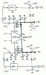
OK, here is a schematic to start you off (see attached pic).
Note diodes between +Vp and +Vs, also -Vp and -Vs, they are marked 'SD' and 'ZD15-18' on the diagram.
'SD' are schottky diodes, 50V/1A is sufficient. ZD are 1-1.5W zener diodes for 15 to 18V.
C1+C2, C4+C5 are Vp decoupling caps, C4+C3, C7+C8 are Vs decoupling caps - as per TDA729x recomended applications in the datasheet.
The diodes D1,2,3 and 4, marked with *, are optional, and depend on the type of voltage regulator used for +Vs and -Vs. The particular ones I used do not require any extra diodes at all.
CF1 and CF3 are power supply filter caps for Vp, CF2 and CF4 for Vs. In my version of the amp, the input to the regulators is generated by a voltage doubler circuit from the same transformer winding as Vp (this circuit is acvtually a bunch of extra diodes and capacitors). The high voltage that is generated this way (58V) provides a lot of headroom for additional optional filtering and regulation, which easily filters out all Vp power rail nosie, preventing it from getting to the Vs pins.
You can of course derive Vs differently, even using a completely independant transformer. Just keep in mind that the 'SD" and 'ZD' diodes set up certain limits to what the actual voltages can be.
The 'SD' diodes insure that minimum Vs is 0.4V or so less than Vp. If the Vs supply falls below tis, the diodes condoct and connect Vp to Vs.
The 'ZD' diodes insure that maximum Vs is 15-18V more than Vp. If Vp falls below this limit, the diodes conduct and conenct Vp to Vs through a 15-18V voltage drop. This should ideally only happen at power-up or down, when the amp is muted or in standby. It is expected that the +Vs power supply is of limited capacity (only a few mA are needed, you could power many TDA729x Vs lines with a small power supply), so it is important that failure of Vp supply does not result in Vs supply trying to drive the load, without somne form of current limiting (otherwise the Vs supply and/or ZD diodes will be damaged). In my application, this was handled by including resistors in the voltage doubler circuit, there are many alternative ways to insure this.
Finally, your Vs supply may be unregulated, but it must be well filtered. Just be carefiul that it never exceeds Vp voltage by more than 20V, and does not exceed 40V, which is the maximum for the TDA7294. Also, it has to be at least 7V more than Vp if you want to eliminate the bootstrap capacitor (see next post).
Attachments
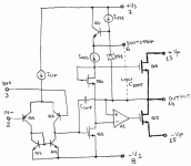
Regarding bootstrap and how it works, a simplified schematic of the internals of the TDA7294 is attached below.
The particular uoutput stage used in the TDA7294, requires that the gate voltage for Q8, be higher than +Vp if the output voltage is to reach close to +Vp (this is required for maximum output power and efficiency, hence, least heat and maximum output for given Vp supply voltages). In particular, about 7V higher voltage than +Vp is required to be able to 'swing' the output voltage all the way up to +Vp. (the negative swing has no such limitation, as Q9, responsible for it, is driven differently).
If you look at the schematic, you will see that the gate of Q8, conencts to +Vs, through Q7, and a constant current source, Ivas. If the output was at the same potential as +Vp, the gate of Q8 would need to be higher than +Vp by the voltage drop on Q6 - this will be about 5V - but, in order to have a voltage drop on Q6, the current Ivas, has to be flowing through it. And, in order for this to happen, the voltage drop on Q7 and Ivas must be more than the minimum required for them to work, about 2V. And, for all of this to be satisfied, it comes out that +Vs must then alwys be at least 5V (for drop on Q6) + 2V (for drop on Ivas and Q7) = 7V higher than +Vp.
Now, if you look at the application for the TDA7294, you will see that +Vs and +Vp are connected together. With no extra measures, this would mean that the output voltage could never become higher than +Vp less 7V - as an example, at +27V Vp, this would mean a reduction in output power from 45W into 8 ohms, to 25W into 8 ohms, yet the amount of heat produced by thie '25W' amplifier would be the same as for the 45W one! What is worse, the output could go up to 20V, but down to -27V, which emans HIGHLY asymetric clipping, which not only sounds horrible, but if sustained, will burn out the speakers due to the asymetric clipping producing a DC component to the output signal.
So, how did they fix this problem? By use of the bootstrap capacitor, and components Q7, ZD1 and Izd1. Their role is to present a voltage roughly equal to the zener voltage of ZD1, between the output and the bootstrap pin, where the bootstrap capacitor is conencted. When the output then swings close to +Vp, the rise of the output 'takes te bootstrap cap with it', maing the cap act as a sort of battery. This 'battery' provides the extra voltage needed over that on +Vp, since the output can now go all the way up to +Vp, and the bootstrap pin is always Vzd1 higher, the bootstrapping provides the extra voltage needed for Ivas and Q6 to work. When the output drops to +Vp less the zener voltage of ZD1, Q7 turns on and replenishes the charge in the boot capacitor.
IMPORTANT!!!
This version of the internal schematic shows that, contrary to what I said two poast above, the bootstrap pin (6) MUST NOT be connected to the +Vs pin (7) as this may destroy Q7 by reverse breakdown of it's B-E junction!!!
I have seen a version of the schematic where there is an additional diode between Q7 and the bootstrap pin, however, since this cannot be verified, it is safest to keep the bootstrap pin open when the bootstrap cap is not in use.
To sum it up, IF +Vs can be kept at least 7V higher than +Vp, the bootstrap capacitor is not needed, as the higher +Vs insures that Ivas and Q6 work through Q7 anyway. In all other cases, you must use the bootstrap capacitor to insure full output power, symetric clipping and therefore maximum efficiency and reliability, as well as minimum distortion.
Final note: Strictly speaking, -Vs does not need to be lower than -Vp, however, it shold never be higher due to chip manufacturing issues already discussed (if it gets more than some 1V higher, the chip latches up and becomes a short from +Vp to -Vp, and destroys itself spectaculairly).
That being said, filtered -Vs is of great benefit to power supply artifact rejection by the TDA729x., so -Vs should at least be well filtered. In order to simultaneously insure good filtering, and -Vs at least equal or lower than -Vp, it is best to have a few volts 'headroom' between them, which is easyest to accomplich by keeping -Vs below -Vp. Also, because most parts in symetric positive and negative regulators are the same, it is easyest if + anbd - Vs are of sme magnitude. Since +Vs is best set 7-8V above +Vp, this will also make -Vs 7-8V below -Vp.
Attachments
Thank you again for a very detailed explanation - now everything became clear.
So perhaps I'll take the +-Vs from a separate transformer winding (it is around 90V rectified) and regulate it a bit, maybe to +-40V. Then put schottky and zeners between Vp and Vs according to your schematic, take out the bootstap cap and leave the bootstrap pin open.
Earlier I thought, that all the internal circuitry, except output transistors would require between 5 to 10 watts, but I was mistaken So, no need for separate traffos 🙂
And maybe one final question - what specific parts would you suggest for regulating Vs? Are LM317/LM337 enough, or are there some better alternatives? And regarding schottky diodes - perhaps I should use the ones with the lowest possible forward drop voltage?
... and one more thing - do I need to place decoupling caps on Vp as close to the chip as possible, or it's enough to do with Vs.
Regards, Artiom.
So perhaps I'll take the +-Vs from a separate transformer winding (it is around 90V rectified) and regulate it a bit, maybe to +-40V. Then put schottky and zeners between Vp and Vs according to your schematic, take out the bootstap cap and leave the bootstrap pin open.
Earlier I thought, that all the internal circuitry, except output transistors would require between 5 to 10 watts, but I was mistaken
So, no need for separate traffos 🙂And maybe one final question - what specific parts would you suggest for regulating Vs? Are LM317/LM337 enough, or are there some better alternatives? And regarding schottky diodes - perhaps I should use the ones with the lowest possible forward drop voltage?
... and one more thing - do I need to place decoupling caps on Vp as close to the chip as possible, or it's enough to do with Vs.
Regards, Artiom.
u can refer to the Velleman K8040 kit instruction on how to implement the diff V supply to the tda7293
http://www.designnotes.com/downloads/Manual_K8040.pdf
http://www.designnotes.com/downloads/Manual_K8040.pdf
Fossil said:u can refer to the Velleman K8040 kit instruction on how to implement the diff V supply to the tda7293
http://www.designnotes.com/downloads/Manual_K8040.pdf
No you can't because they use the same for both Vp and Vs - you should have given the schematic a closer look, the resistors between Vp and Vs are actually zero ohm jumpers. Replacing the one on the negative side with anything much higher will destroy the chip due to latchup on initial power-up.
ArtiomR said:Thank you again for a very detailed explanation - now everything became clear.
So perhaps I'll take the +-Vs from a separate transformer winding (it is around 90V rectified) and regulate it a bit, maybe to +-40V. Then put schottky and zeners between Vp and Vs according to your schematic, take out the bootstap cap and leave the bootstrap pin open.
Yes, something like that. But it is easy to make a voltage doubler that will simultaneously give you 2xVp as the inputs to the Vs regulators, you need 3 caps (2x small, 100u, 1x larger 470u), and 4 diodes (1N400x) per side. The nice thing is, you need no extra windings. Of course, if you already have them, you can use them.
Earlier I thought, that all the internal circuitry, except output transistors would require between 5 to 10 watts, but I was mistaken
Even less, I think it's only about 20mA maximum for Vs.
And maybe one final question - what specific parts would you suggest for regulating Vs? Are LM317/LM337 enough, or are there some better alternatives?
LM317/337 may get complicated due to a potentially too large input to output difference at power up. LM3x7 can only take 40V, if you have 90V at input, and 40V at output that is already too much, but even worse, at power up, LM3x7 needs to charge up the decoupling caps for Vs so you may end up with the whole 90V across it, and LM3x7 goes POOF!!!
I used simple two transistor discrete regulators.
Keep in mind +-40V is the absolute max +-Vs for the TDA7294 (+-50 for the 7293), I would keep a few volts away from that, so +-37-38V.
And regarding schottky diodes - perhaps I should use the ones with the lowest possible forward drop voltage?
Not needed, any schottky will already be more than adequate. A normal PN diode may also be adequate but it is cutting it close - I did initially try it only with the zeners (they work as normal diodes in the forward polarized mode) and it was OK - since that was based on the 'high efficiency' application in the TDA729x datasheet, where they used fast PN dioses, not schottky, but since I had schottky diodes, I decided to play it safe and use them. You just must not go over 0.7V difference, and a schottky will typically be half that. Also, -Vs is crytical, +Vs is not, there even a normal diode is used.
... and one more thing - do I need to place decoupling caps on Vp as close to the chip as possible, or it's enough to do with Vs.
Regards, Artiom.
Vp is not as crytical but you should try to place it as close as possible to the Vp pins. The small 100n or so should be as close as possible, electrolytics can be further. Some of the 729x circuitry is also powered from +-Vp although that is not shown in the simplified schematic. In particular, it is the standby section, and the protection, so better play it safe and avoid any potential problems if you can.
Yes, this time I will use the spare windings, but thanks for the suggestion, it may help to save some $ 😉 And are the voltage doublers as easy as this?Yes, something like that. But it is easy to make a voltage doubler that will simultaneously give you 2xVp as the inputs to the Vs regulators, you need 3 caps (2x small, 100u, 1x larger 470u), and 4 diodes (1N400x) per side. The nice thing is, you need no extra windings. Of course, if you already have them, you can use them.
http://hyperphysics.phy-astr.gsu.edu/Hbase/electronic/voldoub.html
Don't know, why they did put + near one end of winding...

...
I've somehow forgotten, that LM317/LM337 can't handle that much voltage
 Could you give me some link about the discrete regulators, as I don't know how to "make" even them. And what types of transistors are "enough" in this application?
 ...
Ok, so we are safe with diodes as long as they are schottky. Then I have one more question - where to put them(and zeners) physically? May I just put them somewhere in the circuit away from TDAs, or they should go close to supply pins? This is important, because isn't much space around supply pins, only for local decoupling with small caps.
Thats all for now, hope soon I will make this "little tweak", and I feel it is worth this little effort 🙄
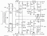
Diodes can be located further from the chip - mine are in the power supply, which is on the same board as the rest of the circuit, but about 10cm worth of wires from it to the actual amplifiers. I have attached the schematic below.
You can see how the voltage doublers are made, using 4x 1N4004, and two caps. The 56 ohm resistor is a small refinement to filter out diode commutation spikes, and drop some voltage (about 2-3V). A single supply is used for both channels.
Note that the BDX53/54 darlingtons have integrated reverse diodes so the extra diodes I gave in the principle schematic are not needed (they are already in the BDX53/54). Of course, you could use different parts, they need to withstand 80V worst case (in practise it will be about 20V) because of initial cap charging and (heaven forbid) short circuits.
Attachments
Thanks for the schematic, you seem to draw them realy fast! 😀
And one more question - how are the output voltages of these regulators calculated? And do I need to change anything apart from removing voltage doublers to make the regulators work out of +-45V?
And one more question - how are the output voltages of these regulators calculated? And do I need to change anything apart from removing voltage doublers to make the regulators work out of +-45V?
Replace the 27k resistors with 33k, and you will get +-43.5V on the regulator outputs. If you also remove the 470k resistors, you will get about +-47V.
Keep in mind that if your rectified DC is 90V CT (+-45V) you have to give the regulator some headroom to regulate - depending on the voltage droop at full load, you may not be able to get even 40V regulated output.
Also, if your +-Vp is +-27V, increasing the +-Vs to over 35V will not have any additional advantage, so you may want to keep the regulators as they are, or just remove the 470k resistors and get about +-39.5V out.
Yes, I already know about a headroom 😉 I'll leave the regulators as in your schematic (+-35V?).
Also I'll put some more capacitance before regulators - 4700mkF per rail, and 2200mkF after them.
Still didn't get all the parts - looks like no one has schottky diodes in quantities of 4 or more atm. Will have to wait until next week, however I already have most of the parts.
I'm just curious, what power rating resistors to use across the regulators? Is 0,125W enough? I usually use 0,5W or more, but the ***tard in a shop gave me those 0,125W, maybe need to get 0,5W ones... 😕
Also I'll put some more capacitance before regulators - 4700mkF per rail, and 2200mkF after them.
Still didn't get all the parts - looks like no one has schottky diodes in quantities of 4 or more atm.
Will have to wait until next week, however I already have most of the parts.I'm just curious, what power rating resistors to use across the regulators? Is 0,125W enough? I usually use 0,5W or more, but the ***tard in a shop gave me those 0,125W, maybe need to get 0,5W ones... 😕
ArtiomR said:Yes, I already know about a headroom 😉 I'll leave the regulators as in your schematic (+-35V?).
Also I'll put some more capacitance before regulators - 4700mkF per rail, and 2200mkF after them.
+-38V (says so right in the schematic).
No need for extreme values of caps. especially in front of the regulators, for two reasons:
1) The +-Vs current drain is only a few mA
2) The output impedance of the regulator dominates any low impedance of the capacitors in front. I did not put 470uF there for nothing, you know 🙂
Large caps on the output are also a dubious proposition, as I said, it's only a few mA, yet, it takes quite a lot of current for the initial charging, and the regulators are NOT short circuit protected (keep in mind that at initial charge-up, output caps behave as short circuits in the beginning!). In case +-Vp drops more than 15V below +-Vs, the regulator output caps are discharged into the +-Vp caps via the zener diodes, no current limit. Again, big caps to discharge means lots of current, and may mean dead zeners.
Of course, you do need lots of capacitance for the +-Vp power supply.
You have to be careful to understand all aspects of a circuit operation, not just 'normal' but also the transient behaviour at power up and power down - before you go changing things.
BTW as drawn, the output of the regulator shows less than 2mV AC component that looks like the input signal, at full output power - this is >2000-fold improvement over directly coupling Vs and Vp. Bigger caps are unlikely to signifficantly affect this, in fact, you may make things slightly worse as what you are after with reg. output caps, is low ESR at high frequencies, where the TDA729x power supply rejection is worse. Large caps tend to have lower resonant frequencies (where ESR is lowest) and may have higher ESR at frequencies of interest.
I'm just curious, what power rating resistors to use across the regulators? Is 0,125W enough? I usually use 0,5W or more, but the ***tard in a shop gave me those 0,125W, maybe need to get 0,5W ones... 😕
All resistors with no markings for power can be 1/8W. Only the 56 ohm ones in the doubler have to be 1W, but you are not going to be using these anyway in your version.
Hi, ilimzn
Made a regulator according to your scheme, and it works! 😀 Took me 4 hours of hardwiring on perforated board(don't know how it's called in English )
Got +-38V at the outputs, one around 0.4V less than other... maybe it's due to resistors tolerances (used standard 5%)?
The problem is, I have almost no headroom for regulation 🙁 I get +-40V after bridge and smoothing caps. For now I've put an old regular bridge, which I will replace with schottky's, this should give a little voltage headroom, but of course not much 🙁 Maybe I should lower the output voltage a little, maybe to +-35V and what values should I change for this?
Didn't wire the regulator to Vs yet... maybe will do it tomorrow.
Made a regulator according to your scheme, and it works! 😀 Took me 4 hours of hardwiring on perforated board(don't know how it's called in English
)Got +-38V at the outputs, one around 0.4V less than other... maybe it's due to resistors tolerances (used standard 5%)?
The problem is, I have almost no headroom for regulation 🙁 I get +-40V after bridge and smoothing caps. For now I've put an old regular bridge, which I will replace with schottky's, this should give a little voltage headroom, but of course not much 🙁 Maybe I should lower the output voltage a little, maybe to +-35V and what values should I change for this?
Didn't wire the regulator to Vs yet... maybe will do it tomorrow.
You need to reduce the 470k resistors, or remove them and replace the 27k resistors with 22k. The latter mod will give you about 34V on the output.
Just replacing the 470k resistors with 220k will give you about 36V on the output.
Also, if the difference between input and output is small, 3-5V, you may need to reduce the 3.3k resistors between the base and colector of the BDX53/54 to 1k or 820 ohms, to give the zener diosed proper operating current. The difference in voltae you are seeing is most likely because of the tolerance of the 10V zener diodes, but 0.5V is normal and not excessive.
Yesterday I've finally connected one channel to the new supply. Everything worked from the beginning, nothing burned or exploded 🙂 For now I've left one channel in old configuration, with shared supply.
From comparing both channels I liked the old one more - it sounds more "natural" and "full-bodied", maybe because of more bass. The new configuration sounds more "dry", with a little less bass, and probably more distortion in midrange. Probably I need to experiment with local bypassing...
The current configurations are:
Old: 5500mkF in supply + 3300mkF Elna RJH on amp board (4-5cm from chip) + 220mkF Sanyo MV-AX on chip pins, all per rail.
New: the same in supply and on board regarding Vp, but I've moved the 220mkF to Vs, also put them on pins, and replaced them on Vp with 47mkF (Sanyo MV-WX). Also I didn't put any fims on Vs near chip pins, as there is not much place... There are only 1mkF polyesters on Vs regulator board.
What are your thoughts?
or exploded 🙂 For now I've left one channel in old configuration, with shared supply. From comparing both channels I liked the old one more - it sounds more "natural" and "full-bodied", maybe because of more bass. The new configuration sounds more "dry", with a little less bass, and probably more distortion in midrange. Probably I need to experiment with local bypassing...
The current configurations are:
Old: 5500mkF in supply + 3300mkF Elna RJH on amp board (4-5cm from chip) + 220mkF Sanyo MV-AX on chip pins, all per rail.
New: the same in supply and on board regarding Vp, but I've moved the 220mkF to Vs, also put them on pins, and replaced them on Vp with 47mkF (Sanyo MV-WX). Also I didn't put any fims on Vs near chip pins, as there is not much place... There are only 1mkF polyesters on Vs regulator board.
What are your thoughts?
- Status
- Not open for further replies.
- Home
- Amplifiers
- Chip Amps
- Tda7293v