the voltage reference wire from Signal Ground to Power Ground must not create a "new" loop.
AND
that ref wire must not connect to the PSU Zero Volts between the smoothing capacitors.
This layout design has improved THD compared to the first one. Tomchr proved it with measurements. I also don't like the long GND lead because it carries the feedback current. (1,07 mA from the first schematic).
I don't know why my png's open to full page.
The ref wire carries current. That was something I had not realised.
That current has a matching partner.
The ref wire MUST FOLLOW the matching partner.
Think for a moment about speaker current.
The PSU sends current from +ve to amp, through amp, to output terminal, through the Flow wire to speaker, through speaker, through the Return wire, across the amplifier PCB tracking close to and parallel to the main PCB traces to the reach the Power Ground Terminal, then continues it's route along the PG wire to the PSU Zero Volts.
The Flow Route from +ve to speaker must be close coupled to the Return Route from Speaker to Zero Volts and into the PSU capacitors to the starting +ve.
This is a quite tortuous route, but for least interference must be adhered to.
The same logical thinking of ALL Flow and Return Routes can eliminate ALL the major and minor interference effects, leaving only microscopic levels.
I think this is what Tom discovered in the P2P comparison to the PCB version.
Tom got some results that bettered the National's specifications. That is very unusual and points to National's LAYOUT not being optimum. When I see some of National's basic errors in the datasheets I can believe they got layout wrong, i.e. worse than not optimum.
Last edited:
###The ref wire carries current. That was something I had not realised.#####
That was the point I was trying to make from the start.
If we only look at the current flow, the first layout should be best and it works for the output and PSU layout. For the chip's inputs, which are voltage driven, it doesn't give the best result. I think it must be more important to have the inputs measuring voltage relative to the same point (input ground) than the current flow to power ground.
Attachments
Yes, I agree.
The amplifier measures the voltage difference across the RCA/XLR input socket.
And processes that signal.
Everything we do in wiring up the amplifier should try to preserve the integrity of that input signal.
That means interference should be minimised everywhere.
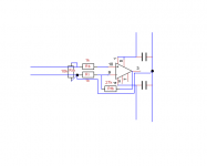
The new route for the ref voltage follows closely along side the input wiring and alongside the chip and alongside the output wire.
But I still don't like the way you are showing the smoothing cap link as the Main Audio Ground (MAG).
Could you separate the MAG from the PSU Zero Volts with a short wire?
BTW, this latest attachment opens in the same page.
What did you do different?
Or is it the Forum Software that determines how we see attachments?
The amplifier measures the voltage difference across the RCA/XLR input socket.
And processes that signal.
Everything we do in wiring up the amplifier should try to preserve the integrity of that input signal.
That means interference should be minimised everywhere.
The new route for the ref voltage follows closely along side the input wiring and alongside the chip and alongside the output wire.
But I still don't like the way you are showing the smoothing cap link as the Main Audio Ground (MAG).
Could you separate the MAG from the PSU Zero Volts with a short wire?
BTW, this latest attachment opens in the same page.
What did you do different?
Or is it the Forum Software that determines how we see attachments?
Last edited:
Pairing wires with the Flow and Return currents matches the CURRENTS exactly.
The pair is a good way to transfer the voltage difference to a new location without extra interference, because the fields of the Flow and Return currents match.
The pair can transfer the required voltage AND give low LOOP AREA.
If there is an offshoot that carries part of the current, then that offshoot must follow the current route that led to the offshoot. Your last diagram shows that. The offshoot (the ref wire) has doubled back along the line of the signal pair.
CAUTION! HAZARD!!
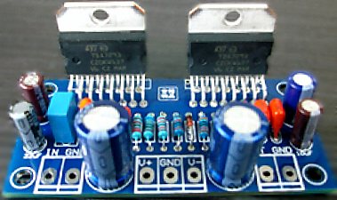
In regards to the schematics at Post#114, Post#118, Post#123, the pinout is incorrect and will cause our TDA7293 amplifiers to explode.
Our board looks like this, with thirty pins total, and eleven are for power.
It doesn't work with the schematics at Post#114, Post#118, Post#123.
P.S.
If the schematics that you post don't apply to TDA7293, then please label them as to what they're for.
Last edited:
In regards to the schematics at Post#114, Post#118, Post#123, the pinout is incorrect and will cause our TDA7293 amplifiers to explode.
as i mentioned in post 105, they are attempting to import into this (TDA7293) context the lessons from Tom's excellent work (on LM3886 layout). the pinouts shown in 114, 118, 123 are LM3886. unfortunately the schematics in those posts do not state that they are for LM3886.
Sorry Daniel, the schematics are directed to the this thread and only because sfthurber was looking for info on PCB design.
http://www.diyaudio.com/forums/chip-amps/252436-lm3886-pcb-vs-point-point-data-3.html#post3846783
Can be converted to TDA7293 or any other chip. Tomchr's made 7 different prototypes, all with the same components. The best version outperformed the data sheet THD+N spec.
http://www.diyaudio.com/forums/chip-amps/252436-lm3886-pcb-vs-point-point-data-3.html#post3846783
Can be converted to TDA7293 or any other chip. Tomchr's made 7 different prototypes, all with the same components. The best version outperformed the data sheet THD+N spec.
yes. my original issue was whether it works to have the ground end of the FB loop (indeed the entire FB loop) near the chip face. that led to a review of Tom's findings. so by degrees we veered off into things for which the context may not be clear to others. sorry about that.
It is good to relocate the -in resistor (~730R), under board, in a direct path from the -in pin to the "free" end of the fb-shunt coupling cap, and then it is also possible to connect the +in load resistor (~22k) from the +in pin to the ground side (0v) of the fb-shunt coupling cap. When those resistors are on both sides of the fb-shunt coupling cap, the groundpoint for both inputs becomes unified. I have not tested that mod with this board.in trying to import tom's results to this (7293 board) context we face the additional uncontrolled variable that the grounding scheme here does not appear to me to closely resemble anything tom tested. for example, (ignoring the slave for a moment) consider the trace beginning at master pin 4, progressing to pin 1 then to the standby cap return then to the NFB shunt cap return then to the input ground then to the rails ground then to the output ground.
As with any mod concerning TDA7293, it is a useful mod when/if it has promoted stability enough to allow setting the gain lower without incurring either instability or any practicality shortfalls in performance. At least the limiting factors are informative.
P.S.
We do already have a board. However, if we did happen to start a new board layout, it would be, necessarily, because of the needs of the chip that it supports, and if that is TDA7293, any new layout would begin with the electrolytic power decoupling caps set as close as possible to pins 7 and 8, to help stabilize the voltage amplifier. Logically, that layout also has a short length 0v trace going over to pin4 for small signal ground, and likewise another 0v trace going in the opposite direction over to run parallel with pin14 for speaker output. So, if you happen to be making or shopping for boards to support TDA7293/4/5/6, that's what you're looking for.
Last edited:
Are you referring to pics in posts 114 & 118 as being better?
No, 114 has the shortest return, so could be expected to be the best option, it is not.
My comments on the inputs were about both of the inputs.
post114, on some other page so I'm going by memory, has invented big new loop areas.
I can see immediately that it cannot perform properly.
Electrically it looks perfect, because we assume wires have no resistance/impedance and that there is no interference going on.
Practically it is just wrong !
This loop area thing is really important.
I can see immediately that it cannot perform properly.
Electrically it looks perfect, because we assume wires have no resistance/impedance and that there is no interference going on.
Practically it is just wrong !
This loop area thing is really important.
I think if I printed off post114 and compared it to post123, the two would appear to be electrically identical.
But loop areas in post123 have been massively reduced by making the wires FOLLOW the current routes.
But loop areas in post123 have been massively reduced by making the wires FOLLOW the current routes.
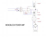
######But I still don't like the way you are showing the smoothing cap link as the Main Audio Ground (MAG). ######
Each bypass cap has its own floating PSU. No need for a MAG, there are no charging currents though the power GND point.
Each bypass cap has its own floating PSU. No need for a MAG, there are no charging currents though the power GND point.
post114, on some other page so I'm going by memory, has invented big new loop areas.
I can see immediately that it cannot perform properly.
Electrically it looks perfect, because we assume wires have no resistance/impedance and that there is no interference going on.
Practically it is just wrong !
This loop area thing is really important.
Post 114 could be made with a small loop areas and still would not be as good as post 123 with its better input layout.
are you confirming that the two caps shown are not the smoothing caps in the PSU?######But I still don't like the way you are showing the smoothing cap link as the Main Audio Ground (MAG). ######
Each bypass cap has its own floating PSU. No need for a MAG, there are no charging currents though the power GND point.
If so then I suggest they are the local decoupling, with the joint representing the on PCB Power Ground.
Is that the case?
the post 139 schematic reminded me of another aspect of chipamp design that i've wondered about. the schematic is agnostic about whether the amp is operated inverting or non-inverting. now then, i've noticed that non-inverting chipamp designs typically include a DC blocking cap in the FB shunt while inverting types typically do not. i don't quite see the reason for this difference in design practice.
the post 139 schematic reminded me of another aspect of chipamp design that i've wondered about. the schematic is agnostic about whether the amp is operated inverting or non-inverting. now then, i've noticed that non-inverting chipamp designs typically include a DC blocking cap in the FB shunt while inverting types typically do not. i don't quite see the reason for this difference in design practice.
sorry, never mind that question, after drawing the circuits both ways with caps it's obvious that with an inverting design an input blocking cap kills two birds with one stone: (1) isolating any DC from the linestage (2) setting the chipamp DC gain at unity.
- Home
- Amplifiers
- Chip Amps
- TDA7293 Parallel kit from ebay (modular/slave style, no lossy emitter resistors)