This should work good and gives enough power
Thanks, brucetassin. I will check, whether they ship to my country.
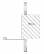
Dear davidus, I'm quite certain that the layout is *electrically* fine (didn't really check it though) but there's a *practical* problem with it: you need the back side of the TDA2005 free for the heat sink .
1) you put R4 there.
2) even if you put it below, as suggested, the chip back is still too far away from the PCB edge, complicating *a lot* heatsink mounting.
If you put the heatsink on top of the PCB, how will you mount it?
And heatsinks are, by definition, heavy; if all that holds it there are the TDA2005 legs, they will soon crack.
My (and all commercial ones) design puts it right on the edge, so it can be bolted to a chassis mounted heatsink or an aluminum back panel.
I use it bridged, but for Stereo PC speakers fed from nominal 12V supplies , I use a dual TDA2003 PCB (a TDA2005 is basically 2 x TDA2003 inside the same case).
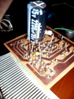
When I get a camera I'll post a couple pictures
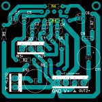
JMFahey, thanks for your valuable advises. Today I got some free time and designed a new layout (with star ground). Here it is.
I want to solder power supply caps (C*-2200uF and C12-0.1uF) directly to IC's pins, at the back side as Gootee advised.
I moved components and let the back side of the chip as free as possible. Regarding the heatsink, I think there is no problem with putting some peaces of plastic between the PCB and heatsink and screwing PCB through them, so the heatsink will be lifted by a couple of millimeters from PCB, and the solder pads of R4 will not touch it. As I'm going to put all these goods in the speaker enclosure, I will cut perfect fit rectangle in the back side of enclosure, so the whole weight of the heatsink will lay on 8mm MDF back panel.
What you think, will it work?
Regards,
David.
Attachments
Last edited:
My bad, I didnt read carefully.
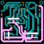
Here it is.
C12 will have to go directly between pins 9 and 6!
C* should connect the same way. But having the short path for that one is not quite as important.
Since c* probably cannot go directly between pins 9 and 6, you should try to add 220uF to 470uF (or more) from pin 9 to pin 6. It could go under the board, if necessary. Try to use the largest capacitance that will fit. Even better would be to use more than one smaller value in parallel, instead of just one larger cap.
Since c* probably cannot go directly between pins 9 and 6, you should try to add 220uF to 470uF (or more) from pin 9 to pin 6. It could go under the board, if necessary. Try to use the largest capacitance that will fit. Even better would be to use more than one smaller value in parallel, instead of just one larger cap.
There is nothing impossible 😀
This is an old PCB that I made last month with different schematics. On final version I will shorten leads of caps and bend large cap under the PCB.
Regards,
David
P.S. By the way, what can you say about the layout that I uploaded yesterday? Is it better than previous one?
Attachments
Last edited: