Lumba Ogir said:ilimzn,
Yes, you have made an amazingly right observation - in other words: maximal correction, all kind, in signal processing and thermal control, is achieved when the driver`s input is directly referenced to the output of the output device, thus 100% feedback is used and we have got an emitter follower...
Also, the local negative feedback is very much faster than the global negative feedback, where the delay can cause serious inaccuracy and harm.
Exactly, it is 'obvious'. However, this does not help us with the task at hand - making a CFP with gain. The trick is in the amount of gain versus the emitter degeneration of the output transistors. Emitter degeneration is a form of local feedback as well, so the thermal dependancy of Vbe of the outputs is reduced, as seen by the driver transistors. A higher gain requires more degeneration - and obviously, this way most of the gain falls to the drivers, because degeneration lowers the gain of the outputs. This is a delicate balance.
Someone mentioned error correction - it is possible to slightly modify the CFP and achieve that as well. In the same manner it is possible to merge a diamond buffer and a CFP to make a very high input impedance buffer, which is thermally stable as long as the diamond buffer is. The CFP is a very versatile building block...
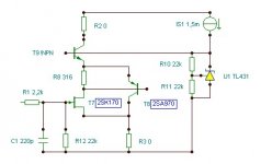
Hi,Lumba Ogir said:Linear cascoded CFP input stage
thanks for that diagram.
I see r2=r3=0r0.
What options for these two resistors work, if the arrangement is duplicated into and LTP?
Does the 170 work properly if r3 is increased to give source degeneration?
What load (r2) does the cascoded CFP expect to see?
What is the optimum (or range of optimum) currents in the FET and the BJT?
Andrew,
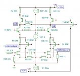
The input stage in post #41 can form a complete power amplifier along with an output stage, like the one in post #35, when sound quality has number one priority. No further stages are necessary. It should have separate, well-filtered and regulated supply.
Here is a very flexible and tunable LTP version:
The current of the J-FETs is set by R8 and R9, like T3Vbe/R8=2mA so the current in T3 and T4 is 3mA.
The gain with current mirrors solely can be considered as too high, is lowered by R12.
Attachments
ilimzn,
Something more serious: bipolar transistors suffer from considerable turn-off difficulties in this position. The resistors worsen it further by delaying the discharge of the base. It remains a problem in any case, can be acceptable as best if the value of the current source resistor is low enough.
(There is no need for emitter degeneration resistor when one output device used, just required for more equal current sharing.)
Lumba Ogir said:ilimzn,
Something more serious: bipolar transistors suffer from considerable turn-off difficulties in this position. The resistors worsen it further by delaying the discharge of the base. It remains a problem in any case, can be acceptable as best if the value of the current source resistor is low enough.
(There is no need for emitter degeneration resistor when one output device used, just required for more equal current sharing.)
Yes - if the input to a CFP output stage can swing close to the rails, rather nasty overhang can be observed on clipping. However, this is mostly a problem connected with the driver transostors, as they essentially cannot drive the base of the output transistor to a voltage greater than that of it's collector - so this is right at the theoretical limit of saturation. Since beta is still there at this point, the base current is not excessive, the switch-off characteristic of the output transistor will dominate it's behaviour, coupled by the size of the B-E resistor. In contrast, the driver transostors can be driven into DEEP saturation - there is nothing to prevent the base current becoming any value. Clamping the base somehow helps. Also, the choice of a proper previous stage helps as well - it is crucial that it's output current is limited. Something like a LTP VAS would do good here, as the maximum current out of it is limited by it's tail current source.
I plan to build an amp with a Sziklai output stage "similar" to that used in ESP project 3A.
http://sound.westhost.com/project3a.htm
Buy using some rudimentary small-signal analysis i have estimated its open-loop gain to be arround 65 dB's (I don't care if it's 71 or 59) as i plan to drive the output stage from an opamp boasting 140 dB's open-loop gain. Is this a really bad idea?
http://sound.westhost.com/project3a.htm
Buy using some rudimentary small-signal analysis i have estimated its open-loop gain to be arround 65 dB's (I don't care if it's 71 or 59) as i plan to drive the output stage from an opamp boasting 140 dB's open-loop gain. Is this a really bad idea?
Output stage of The Ultimate Suplifier
Why not try the Sziklai output stage of The Ultimate Suplifier? See www.suplifier.nl. You also find there the theoretical notes of these output configuration.
Marc Vi.
Why not try the Sziklai output stage of The Ultimate Suplifier? See www.suplifier.nl. You also find there the theoretical notes of these output configuration.
Marc Vi.
in conclusion ......
often when me , our friend here with the original post , and many others when they post one question about a schematic or a protype produced and problems ocured , real experts come up with many usefull solutions ,many suggestions and so on ......
our friend has a circuit with a Sziklai output stage driven by op amp ..... then our friend VHF comes up with his input coming from a simular thing but with mosfet out puts .....( to me this simply off topic !!!!! ) then so many others with various suggestion related to a lot of things ....
MY POINT :
i think that best for all will be to work on the existing circuit and NOT try to modify that .....thats probably the only way to be able to evaluate the original circuit ...... ( meaning post is getting too long and then info is very dificult to proces andor evaluate )
MY INPUT:
1- i dont like simulators
2- Sziklai output stage is something i like very much .to my understanding it both produces wonderfull sonics and has a better long term stability
3- the 99.9% of amplifiers are sensitive to pcb
ground rooting , symetry , current flows ,signal return path , feedback return path ,local filtering , and some others will make a perfect amp.(in your case also local power supp fro op amp )
finally from personal expirience i can tell you that you have there in the schematic is a perfect working amp meaning that if you copy this to a pcb and follow the above everything is going to be fine .....
Do not expect perfection of this amp since it is designed to preserve a very good ammount of safety while operating in heavy use or abuse
this factor was taken very seriously noticed while this amp was designed ( resistors from drivers to output kill sonics but make the all amp work much more safe )
which will bring us to the final conclusion which is that many nice amps are presented in this forum but very few of them will handle PA or any other abuse .....
we will have to compromise between safety and quality .....
thats all folks
Re: Output stage of The Ultimate Suplifier
FTR I personally do not fully agree with the configuration of the Suplifier output stage, although I admit I have never built one. My reasoning is as follows: Firstly the designer incorrectly states that Doug Self advocates EF output stages because the drivers do not reverse bias. Actually the drivers will reverse bias in both cases (EF or sziklai) but the output device will only reverse bias in the case of EF. This is an advantage because the VAS stage will effectively assist in a faster switch-off of the non conducting rail. In essence the sziklai is superior overall when biased in class A and the EF is superior in class ab. IMO the Suplifier would be a superior class AB amlpifier if the driver stage was configured as class A sziklai and the output devices as class B EF which is almost the reverse of the existing circuit. I have personally built such an output stage and can highly advocate it. The class A sziklai driver stage provides a constant impedance VAS loading and the low output impedance nicely buffers the VAS from gm doubling effects of class AB.
Marc Vi. said:Why not try the Sziklai output stage of The Ultimate Suplifier? See www.suplifier.nl. You also find there the theoretical notes of these output configuration.
Marc Vi.
FTR I personally do not fully agree with the configuration of the Suplifier output stage, although I admit I have never built one. My reasoning is as follows: Firstly the designer incorrectly states that Doug Self advocates EF output stages because the drivers do not reverse bias. Actually the drivers will reverse bias in both cases (EF or sziklai) but the output device will only reverse bias in the case of EF. This is an advantage because the VAS stage will effectively assist in a faster switch-off of the non conducting rail. In essence the sziklai is superior overall when biased in class A and the EF is superior in class ab. IMO the Suplifier would be a superior class AB amlpifier if the driver stage was configured as class A sziklai and the output devices as class B EF which is almost the reverse of the existing circuit. I have personally built such an output stage and can highly advocate it. The class A sziklai driver stage provides a constant impedance VAS loading and the low output impedance nicely buffers the VAS from gm doubling effects of class AB.
Re: Re: Output stage of The Ultimate Suplifier
Can you post a schematic to confirm your description?
I wonder if your description matches the output stage of the Crimson series VIII?VHF man said:IMO the Suplifier would be a superior class AB amlpifier if the driver stage was configured as class A sziklai and the output devices as class B EF which is almost the reverse of the existing circuit. I have personally built such an output stage and can highly advocate it. The class A sziklai driver stage provides a constant impedance VAS loading and the low output impedance nicely buffers the VAS from gm doubling effects of class AB.
Can you post a schematic to confirm your description?
VHF man,
CFP output is of crucial importance, CFP driver/EF output... not that exiting. It is about distortion in the output stage.
CFP output is of crucial importance, CFP driver/EF output... not that exiting. It is about distortion in the output stage.
Guys, thanks again...I must say that I gave up from this project because I never solved oscillations issue. I made 4 amps based on this schematics, and 2 of them worked nicely but burned after 6 months because of heavy load..3 and 4. amp never started working (god knows why....) so I found this too complicated and hard to trust... Thanks anyway 😀
hmmmm
that sounds like the things i was talking about .....will it be possible to have a picture of your pcb or pictures of your final layout ????
i actually seen this circuit before and i felt like playing with it since it is relativelly simple ....also if constructed properly i think its looks solid rock to me
Moby said:Guys, thanks again...I must say that I gave up from this project because I never solved oscillations issue. I made 4 amps based on this schematics, and 2 of them worked nicely but burned after 6 months because of heavy load..3 and 4. amp never started working (god knows why....) so I found this too complicated and hard to trust... Thanks anyway 😀
that sounds like the things i was talking about .....will it be possible to have a picture of your pcb or pictures of your final layout ????
i actually seen this circuit before and i felt like playing with it since it is relativelly simple ....also if constructed properly i think its looks solid rock to me
Originally posted by VHF man
In essence the sziklai is superior overall when biased in class A and the EF is superior in class ab.
What? This is a result from your experiments? What i did understand is that the Sziklai output posed an extra advantage in class B: The crossover region is reduced from 1.4V to 0.7. I even have some UHF video germanium transistors that could bring it down to 0.3 if used as drivers (I know these are leaky and have reliability issues and don't want to go off-topic).
ionomolo said:I plan to build an amp with a Sziklai output stage
//----//
Is this a really bad idea?
It can be a good idea.
I am often using Sziklai, complementary feedback pair, CFP.
There can be issues of oscillation.
But handled correctly to avoid eventual oscillations (which does not often happen, to me)
this way is one good alternative to using a Darlington Pair.
Both Darlington and Sziklai make use of the combination of 2 transistors
to get a high gain 'device'.
It may be very interesting to read this
http://www.dself.dsl.pipex.com/ampins/discrete/cfp.htm
It was from this article, I first learned about
how good this configuration Can Be 🙂
Even compared to 'normal' Darlington.
It is from Douglas Self tutorial
DESIGN WITH DISCRETE TRANSISTORS
* Introduction. (This page)
* How transistors work. (This page)
* Simple emitter-followers
* CFP emitter-followers
* Single transistor gain stages
* Two transistor gain stages
* Discrete opamps
http://www.dself.dsl.pipex.com/ampins/discrete/discrete.htm
😎 😎
Lineup, regars
please moby
except the information given to me about this in PM it would be very nice to present the lay out for others to see and share more opinions
thank you
except the information given to me about this in PM it would be very nice to present the lay out for others to see and share more opinions
thank you
this will be
my approach in an amplifier like that
--- keep amplifiers seperated from each other
----keep amplifiers away from secondary circuits
----since amplifier board requiers only 9x18 cm if 2 of them are fited on the side of a sassi then there is enough space to create one pcb that will include all the secondary circuits like protection ,fan control,secondary psu, mains rectifier and filters .
---- also it can be all done in one pcb but topology should remain the same ( to my opinion )
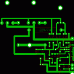
this is a pcb that is designed in 15 minutes but more or less this is the way i like to make them....
next days i will try to shape it abit more and then poduce a protoype to see how its going .....
will post my results ....
my approach in an amplifier like that
--- keep amplifiers seperated from each other
----keep amplifiers away from secondary circuits
----since amplifier board requiers only 9x18 cm if 2 of them are fited on the side of a sassi then there is enough space to create one pcb that will include all the secondary circuits like protection ,fan control,secondary psu, mains rectifier and filters .
---- also it can be all done in one pcb but topology should remain the same ( to my opinion )
this is a pcb that is designed in 15 minutes but more or less this is the way i like to make them....
next days i will try to shape it abit more and then poduce a protoype to see how its going .....
will post my results ....
Attachments
- Status
- Not open for further replies.
- Home
- Amplifiers
- Solid State
- Sziklai output