Hi,
why are the emitters of the drivers loaded with 22r to ground?
This makes the driver stage a power stage?
Surely this is not an efficient way to slug down the drivers to make the circuit stable?
why are the emitters of the drivers loaded with 22r to ground?
This makes the driver stage a power stage?
Surely this is not an efficient way to slug down the drivers to make the circuit stable?
Andrew,
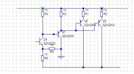
The 22R's are part of a divider, as the CFP has a significant voltage gain.
Moby,
Another thought, make the output devices a darlington, that is connect a driver as a EF driving the outputs, connect the collector to ground, so it can be a lower voltage and lower power device.
This should reduce the drive current so you could use something like 2n5551 / 2n5401 in place of Q1 and Q2.
The problem here is lots of gain, so will require care ...
Sorry, I don't understand😕 Can you draw it?Another thought, make the output devices a darlington, that is connect a driver as a EF driving the outputs, connect the collector to ground, so it can be a lower voltage and lower power device.
Hi,
the driver device has to be selected very carefully for several reasons. High voltage transistors intended for video applications are most suitable for this important and difficult task, with 2pF typical Cob, like BF869/70 but others from Toshiba, Hitachi and especially Sanyo would be better, some of them have excellent linearity too.
The high base-collector capacitance of the output transistor is from stability point of view not a disadvantage.
Symon,
changing the topology is giving up the superior and unique sonic and functional qualities provided by the CFP. (Except the oscillation issue).
Thanks. I'm still searching for the right drivers. maybe mje15033....But Onsemi does not say nothing about capacitance😕
TOINO, what I have to look at QSC schemo. It's real mess on that manual

TOINO, what I have to look at QSC schemo. It's real mess on that manual
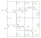
Thanks, now I know what you are talking aboutI've only drawn the top half and didn't correct the component values, but you get the general idea
Hi Moby
I remember that http://www.gbaudio.co.uk/data/1400s.htm amplifier.
The layout is SO CRITICAL that the op-amp circuitry in your sch http://www.diyaudio.com/forums/showthread.php?postid=1277034#post1277034
is placed directly on the output binding-posts!!
This amplifier is really minimalist, and in my humble opinion, the NE5534 has no power enough for that task.
I suggest you try to parallel 2 or more.
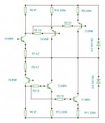
The QSC works like the picture posted by Symon and is a good reference for components.
Note that the drivers are cascodes…
I remember that http://www.gbaudio.co.uk/data/1400s.htm amplifier.
The layout is SO CRITICAL that the op-amp circuitry in your sch http://www.diyaudio.com/forums/showthread.php?postid=1277034#post1277034
is placed directly on the output binding-posts!!
This amplifier is really minimalist, and in my humble opinion, the NE5534 has no power enough for that task.
I suggest you try to parallel 2 or more.
The QSC works like the picture posted by Symon and is a good reference for components.
Note that the drivers are cascodes…
There is a slight difference between my drawing and the QSC output stage. In my version the collector of the output driver is deliberately connected to ground and not the output terminal.
This means that it isn't affected by the extreme changes in collector voltage, and hence changes in capacitance. It can also be a lower voltage device so perhaps more choice?
This means that it isn't affected by the extreme changes in collector voltage, and hence changes in capacitance. It can also be a lower voltage device so perhaps more choice?
Hello all,
remember that, traditionally, the CFP output (or Sziklai), has the collectors of the "dumpers" transistors (the power ones) connected to the emitter of the driver transistor, before the emitter resistor.
In the drawing in the post before mine, T3 and T4 collector should be tied to the emitter end of R7 (and the same thing for the lower half of the output).
Anyone tried using a small (high gain) bjt for driver, then instead of a power bjt, a driver + power bjt (a complete EF output stage)?
Maybe that will be harder to stabilize, because of the 3 bjt in feedback loop instead 2.
Hi all
If you want it REALY simple, and absolutely minimalist: 😀 http://www.qscaudio.com/support/library/schems/Discontinued/USA Series/usa370.pdf
If you want it REALY simple, and absolutely minimalist: 😀 http://www.qscaudio.com/support/library/schems/Discontinued/USA Series/usa370.pdf
Giaime,
yes, I prefer it that way, just had the present design in mind.
T3 and T4 collector should be tied to the emitter end of R7
yes, I prefer it that way, just had the present design in mind.
Attachments
More thoughts about this theme:
The driver and the output device are in tight cooperation using a large amount of local negative feedback.
As the output device will follow the driver, the properties of the driver are decisive, resulting in several remarkable features, like a level of linearity hardly achievable by other means, certainly not with the commonly used output topologies. GNF and obscure error correction techniques can not compete with the CFP.
The driver needs to have some robustness as the output device being slow, it has to supply the load current at high frequencies.
Bipolar driver transistor and fast lateral FET is a nice combination. However in my opinion, the driver standing current should be much higher than widely estimated, about 50mA/500-1000pF Cgd.
Small signal transistors can not provide that at typical rail voltages. Not very long anyway.
That's what I'm takling about😉Bipolar driver transistor and fast lateral FET is a nice combination. However in my opinion, the driver standing current should be much higher than widely estimated, about 50mA/500-1000pF Cgd.
Giaime said:Hello all,
remember that, traditionally, the CFP output (or Sziklai), has the collectors of the "dumpers" transistors (the power ones) connected to the emitter of the driver transistor, before the emitter resistor.
This is an excellent point that many contributors to this thread seem to have missed. If the connection is not done this way, thermal stability becomes dependant on the output transistors, and further, can depend on the temperature of the input transistors times their effective gain. Getting this right is especially difficult with CFP stages with gain. I have some limited experience with this, and for me, selecting the lowest possible gain has worked the best. The reason for this is that the higher the gain, the less the thermal behaviour of the outputs influences the drivers (due to the emitter divisor required for gain, the input transistors see only a fraction of the output transistor current on their effective emitter resistances).
I also have some experience with BJT/MOS CFP. Lateral MOS works great here but almost requires a CFP with gain or you end up with excessive rail voltage loss (normally about 7-8V at full power). One thing that needs careful attention in this configuration is clipping behaviour, especially due to any form of current limiting implemented in the output stage - because the gates of the MOSFETs (unlike BJT bases) don't draw signifficant current, at the point of clipping, the BJTs start conducting all the load current through gate protection zeners (which will, unchecked, result in their quick destruction).
ilimzn,
Yes, you have made an amazingly right observation - in other words: maximal correction, all kind, in signal processing and thermal control, is achieved when the driver`s input is directly referenced to the output of the output device, thus 100% feedback is used and we have got an emitter follower. (That`s why emitter followers are much more linear). But varying Ic and thermal instability of the driver would worsen it.(Separate heatsink required!)
Also, the local negative feedback is very much faster than the global negative feedback, where the delay can cause serious inaccuracy and harm.
- Status
- Not open for further replies.
- Home
- Amplifiers
- Solid State
- Sziklai output