Your vague dislike about phase gain variation of the loop gain makes me guess that you would prefer a more constant loop gain and phase over the entire audio range.
Here a version which would serve this design goal, however it will have much higher THD, but I understood THD is not your concern.
This version should be easy to mod from standard designs with IRS2092.
I have chosen low resistor values in the small signal area. From perspective of IRS2092 you could go for approx 3 times higher resistor values and 3 times smaller capacitances if your layout is good enough.
Attachments

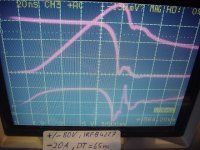
When looking to an output signal of 40Vpk:
With +/-80V rails you need just a moderate modulation of the duty cycle,
but with +/-53V rails you need a massive modulation of the duty cycle in order to achieve 40Vpk.
As a consequence with +/-80V rails the modulator distortions at output signals of 40Vp are much less.
To a certain extend this is also corresponding to the frequency drop at high modulation levels.
IMHO it is hard to read such things from frequency domain.
Not sure if Bruno would agree with me - but to me frequency domain is only helpful for the part of linear control theory. Everything else, including the topic of non linear control theory, I prefer to examine in time domain.
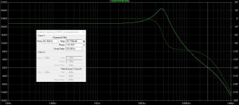
Why does the low frequency have such large gain in the picture 30db ? 😕
...failed to find a picture which fits to your question. Which picture in which post is your concern?..in the picture 30db ?
...failed to find a picture which fits to your question. Which picture in which post is your concern?
Post #602
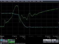
At the start of the sweep there is a massive, what looks like a bell shape curve followed by odd harmonics, then further up the spectrum the points where oscillation seems to start approx 300KHz. Am I correct this is how to read the frequency domain.
Don't bother about the shape of the bells.
That's just an artefact of the FFT in LTspice. The peak of each bell tells
the size of this harmonic.
The shown Spectrum is with an 1kHz sine wave input so we would wish to see only the +29dB at the output of the amp ..., but the amp causes deviations from this signal. It changes the shape, which can be expressed by a sum of multiple sine waves with frequencies that are multiples of the fundamental.
Fundamental with 1kHz is at +29dB, 3rd harmonic shows approx. -32dB.
Means third harmonic is 0.09% of the fundamental.
Fifth harmonic is almost similar in size....
Why? The FFT does not directly tell you why harmonics go up or down.
To find the reasons you have to dig deeper into the circuits.
But for the discussed circuit at medium to large signals most of the distortions are caused by the self oscilating modulator (which is pretty common for phase-shift-delay-self-oscilator-class-d-amps) . Switching frequency is depending on the excitation. With increasing excitation and duty cycle the shape of the carrier is affected, which directly hits into THD. Furtheron the size of the carrier is affected as well, means the gain of the modulator is a function of the duty cycle - means close to the zero crossing of the music signal the system has more loop gain compared to moments where the music signal has its max or min.
Feel free to watch the carrier at the comp pin of the simulation, it will look more or less like a triangle when the input signal is close to zero. With growing input signal it will change the shape and size.
And yes, in the region above 300kHz you see the carrier.
With increasing excitation and duty cycle the shape of the carrier is affected, which directly hits into THD. Furtheron the size of the carrier is affected as well, means the gain of the modulator is a function of the duty cycle - means close to the zero crossing of the music signal the system has more loop gain compared to moments where the music signal has its max or min.
Feel free to watch the carrier at the comp pin of the simulation, it will look more or less like a triangle when the input signal is close to zero. With growing input signal it will change the shape and size.
And yes, in the region above 300kHz you see the carrier.
Thank you for clarifying this, I now have a better understanding on the subject.
Last edited:
D
Deleted member 148505
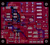
Attached schem with updated values for the gate drive. If anyone wants the gerber, just message me and I will give the file.. Though I have the right to deny the file to anyone, specially those who have dubious looking accounts, I will give it only to DIYers (and not mass producers).
Note: Free gerber is for this specific version only (see attached pic). Also I have other derivatives of the layout and will be for sale and those are not shareable. Thanks!
Note: Free gerber is for this specific version only (see attached pic). Also I have other derivatives of the layout and will be for sale and those are not shareable. Thanks!
Attachments
Last edited by a moderator:
Dependency of the loop gain from supply rails:
Obviously the magnitude of the comparator output is proportionally growing with the rails.
But at the same time also the triangle carrier grows in the same manner.
In equation (4) of Brunos "Simple Self-Oscillating Class D Amplifier with Full Output Filter Control"
you see that both effects fully cancel out.
Also in reality loop gain is stable over a wide range of the rail levels.
Despite the lite amp having different additional transfer functions involved,
the independency of the loop gain from the rail voltage applies in the same manner.
Step response of the complete amp:
In order to reach clipping with same input level, I increased the closed loop voltage gain of the amp,
by reducing the input resistors. There I also increased the low pass cap.
Increase of the chosen low pass cap is slightly more than the reduction of the resistors.
==> Step response is slightly slower, but of perfect shape.
Testing:
High power long term music and short circuiting at high signals are more the things you can do,
after you have finished the R&D work and when you are convinced that it is bullet proof.
Before that - better go through the points below.
Please understand that this is not a full R&D manual, but just a rough overview.
Whenever you observe behaviors, which do not fit to your theoretic expectation or design goals,
then search the error, which can be in the proto and/or your theory.
Every point where you are not able to bring both to identical 'opinions', increases your risk to fail,
but fortunately few open questions do not immediately make success impossible.
Testing / R&D work to be done for 55V:
- Double check if the values in the BOM are making sense from theory:
SIM: Adjust simulation to the new values and see if fs, step response, stability etc fit.
stone age hand calculations: Check if biasing components auxiliary supplies etc. and IR + MosFet specific values including parametrization of dead time and over current do fit.
- Based on the theoretic expectations from above and after setting up the proto check/correct things as below:
In the beginning work with current limited supply (0.5A limitation is a good choice here)
Aux supplies
DC operating points
Basic oscillation
Timings of the gate drive in idle situation
Signal shapes and signal integrity in the small signal area
After all this is fine you can go for a stronger supply:
-Examine switching wave shapes as described below, but stay with load currents around 4A.
-Check the overcurrent protection by using a 50uH+0.1R load and small input signal (anything between 100Hz...1kHz) slowly increasing until
you reach the shut down. If shut down still does not happen at 10% above the desired level - stop and readjust!
Test high side limits independend from low side limits, simply by disabling always the opposite protection.
-After this, recheck switching wave shapes 3) 4) 5) 6) with currents close to shut down.
Examination of switching wave shapes:
Amp without input signal (input shorted).
1) Idle/no load, event of turning off the low side MosFet
2) Idle/no load, event of turning on the low side MosFet
3) Sink load current. Resistor from pos rail to amp output, event of turning off the low side switch.
4) Sink load current. Resistor from pos rail to amp output, event of turning on the low side switch.
5) Source load current. Resistor from neg rail to amp output, event of turning off the low side switch.
6) Source load current. Resistor from neg rail to amp output, event of turning on the low side switch.
Typically, I do not have the load towards the rail connected when staring up the amp, but connect it manual just for the short time of doing the measurement. Easy for the LiteAmp, but for the 2kW monster and involved currents and voltages this game always was an impressive welding event at the contact point.... Better wear glasses.
Alternatively you could use some proper electronic relay, but the arcing during the manual test can also be seen as a ruggedness test.
For measurements 3,4,5,6 start with reasonably small currents, because untamed and badly ringing half bridges will burn at higher currents.
Interesting current levels start when the load current is larger than the filter ripple current.
So measure - adjust - measure - adjust- measure - increase load - measure - ....
If you use an isolated floating power supply, then all this can be done even without the need of differential probes.
Do not try to simulate equivalent situations by applying DC to the amp input with load from amp output to GND. DC signal and load to GND would cause heavy bus pumping!
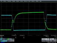
All attached screen shots were taken with the following settings:
Time scale is 50ns per horizontal grid.
Upper trace: Ugs of the low side switch, 5V per vertical grid
Lower trace: Half bridge output voltage, 20V per vertical grid
Hi, Choco,
This is very useful guide to the debug the board, to compare with your waveforms, I also attach some of mine.
The depressed thing is i have big dip of the Vgs once the mosfet turns on in the current source waveform, while the current sink waveform looks ok.
PS:
1. All the waveform are Vgs(green) & Vds(cyan) for lower mosfet
2. Waveforms are: Idel, 20A sink, 20A source
i hope you can give some comments on it.
Thanks,
Attachments


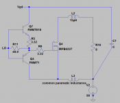
Hi Eric,
it looks like your layout has a certain common source inductance,
more than only the inductance of the lead of the IRFB4227.
Means it looks like you are not running a separate track from the gate drive circuit (IRS circuitry + BJT) to the MosFet, but share a common track of the negative rail for the power current and the gate drive loop.
Nevertheless, with respect to the high currents and tough testing situation the shown waveforms are not bad.
P.S.
In your LT-Spice file I am wondering if there is the GND connection missing for V4 & V5?
Hi Eric,
it looks like your layout has a certain common source inductance,
more than only the inductance of the lead of the IRFB4227.
Means it looks like you are not running a separate track from the gate drive circuit (IRS circuitry + BJT) to the MosFet, but share a common track of the negative rail for the power current and the gate drive loop.
Nevertheless, with respect to the high currents and tough testing situation the shown waveforms are not bad.
P.S.
In your LT-Spice file I am wondering if there is the GND connection missing for V4 & V5?
It does miss the ground connection between the rails, thanks for checking.😀
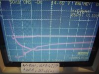
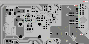
Base on your comments, my layout trace may like the pic in attached. Does this dip peak cause some risks? if this peak voltage does not exceed the Vgs maximum rating, it will be ok? Or can we add the diode(1N4148) the clamp it?
Thanks,
Attachments
At first glance the dip looked larger than what I would expect from inductance of the TO-220. But when looking into numbers, it turns out that this dip theoretically could be already caused by inductance of the IRFB4227.
The dip happens in the moment when the sloping touches the lower rail. While during sloping one can anticipate that the load current will split into the capacitances of both MosFets, at the end of the sloping all current will run through body diode of the lower MosFet. Means in the source leg and the track which carries the load current we will see a current step of approx half of the loaf current.
It is slightly hard to read the ns from your 200ns/grid screen shot but it looks like the dip has a rise time of 20ns. Means di/dt must be approx (0.5x20A)/20ns = 0.5A/ns.
This di/dt causes a dip of approx. 3.5V (from +1.9V down to-1.6V).
==> Common source inductance seems to be around 3.5V/(0.5A/ns)=7ns.
This value would fit more or less to the source lead inductance of a TO-220 with long leads (or short leads + few mm common track in the layout).
I think this peak is uncritical.
The thing which is making me wonder is an older measurement from an halfbridge with IRFB4227, which is not showing much dip. It was measured on a modded LiteAmp board where I had implanted two IRFB4427, just for experimenting direct gate drive of IRFB4227 from IRS2092.
Both screen shots are showing your load situation: Sourcing 20A into a resistor behind the filter to negative rail. But in fact my measurement had a wire loop and current probe inserted in the drain wire of the low side MosFet. This additional inductance combined with the snubber outside of this current loop reduced di/dt in the device. It was around 0.2A/ns (20A/100ns).
In both screen shots below the traces are:
Upper trace: Vds of low side MosFet, 50V/div. (zero level: middle of the screen)
Middle trace: Id of low side MosFet, 10A/div. (zero level: two divisons below middle of the screen)
Lower trace: Vgs of low side MosFet, 5V/div. (zero level: three divisions below middle of the screen)
Time base of first screen shot: 20ns/Div.
Time base of first screen shot: 50ns/Div.
Attachments

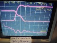
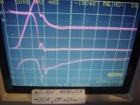
...big dip of the Vgs...
Just double checked your screen shot.
The voltage dip is double of what I had put in my last post.
So it is a 7V dip (from +3.8V down to -3.2V).
This leads to calculated 14nH common source inductance.
Cannot be only the lead inductance.
For a more detailed analysis you would need to disclose your PCB
and also show where&how you connected the probes.
The dip happens in the moment when the sloping touches the lower rail. While during sloping one can anticipate that the load current will split into the capacitances of both MosFets, at the end of the sloping all current will run through body diode of the lower MosFet. Means in the source leg and the track which carries the load current we will see a current step of approx half of the loaf current.
Yes, the dip is right align with the Vds slope to zero, my understanding is that this source current first run through the body diode(deadtime) of the lower Mosfet, once it totally on, the body diode will be bypassed by this mosfet.
if this dip voltage caused by the parasitic inductance of the common source trace, this induced voltage should last more than 20ns ( compare to your pic takes 100ns to decrease 20A to 0)? is there any relation with the upper mosfet?
Your screen shot is very nice, I'll prepare to upload some more for detail discussion.
Thanks again for your kindly reply🙂
I think the di/dt in my set up was slower than in yours.
From the upper MosFet I do not have the counter part signal.
You mean that in my case the upper MosFet might still carry some current also when the halfbridge has already fully sloped to negative rail?
I think yes, this the case.
We can have a look the corresponding situation of the lower MosFet.
The situation of the upper MosFet when turning off at sourcing situation is theoretically the same like when looking to the lower MosFet when turning off in sinking situation.
The attached screen shot shows the turn off of the lower MosFet during sinking.
The voltage is sloping within 20ns, while the current takes about 40ns until it becomes zero.
The trace which starts at the left upper end is the drain current: 10A/div (zero level in the middle of the screen)
The trace which starts at the middle is Vds: 50V/div. (zero level at the middle of the screen)
The lowest trace is Vgs: 5V/div. (zero level is three grids below middle of screen)
Attachments
..my understanding is that this source current first run through the body diode(deadtime) of the lower Mosfet, once it totally on, the body diode will be bypassed by this mosfet.
Basically this is the sequence. For the IRFB4227 at -20A this is mostly valid if the junction is still cold. If the junction is hot, then the resistance of the N channel is not low enough anymore to bypass all current. At the same time the Vf of the diode is lower at high temperatures. As a consequence with an IRFB4227 running in real life at -20A you will get a current sharing between N-channel and body diode.
Just double checked your screen shot.
The voltage dip is double of what I had put in my last post.
So it is a 7V dip (from +3.8V down to -3.2V).
This leads to calculated 14nH common source inductance.
Cannot be only the lead inductance.
For a more detailed analysis you would need to disclose your PCB
and also show where&how you connected the probes.
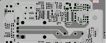
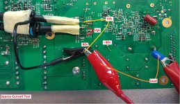
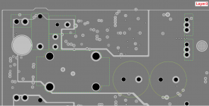
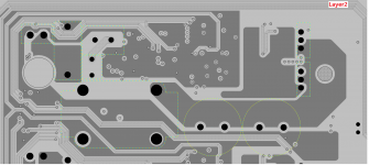
I have put some PCB layouts and the test setting in attached, please help to check it.
Also, the last pic is testing with adding diode clamp between the gate and the source during the source current phase. It looks like this diode clamp works, but we get more peak voltage once the dip rise up.
Thanks!
Attachments

Nice screen shot 🙂
And I agree, your layout does not have much of common source inductance.
This zoom looks like your di/dt are even higher than earlier anticipated.
High di/dt, but well controlled without much ringing.
The fall time to the negative peak is about 5ns, not 20ns as I had anticipated
from the earlier unzoomed pictured.
There you have a pretty fast layout 😀 and in this case I have to revise my 'Cannot be only the lead inductance.'
With such short commutation times and related high di/dt the voltage peaking of the Vgs easily can be caused by the inductance of the source lead.
Furtheron I think you do not need the diode.
-4V appears really uncritical for a MosFet which is specified for +/-30V.
Furtheron the Vgs inside the housing, right at the die will look different.
The internal Rg (not specified for this type, but likely a few single Ohms) together with 4600pF input capacitance will internally further milden such fast voltage peaks.
To me your shown wave form looks pretty OK.
How is turn ON looking during sinking?
Usually turning ON of the low side MosFet during sinking would be the most critical in terms of fast HF resonances and correct adjustment of the snubber.
The attached screen shots show the turn on of the lower MosFet during sinking (-20A) of the modded LiteAmp. First screen shot with 50ns/div, second with 20ns/div.
The trace which starts at the left upper end is Vds: 50V/div. (zero level at the middle of the screen)
The trace which starts at the middle is the drain current: 10A/div (zero level in the middle of the screen)
==> Current peak reaches almost 40A while removing the Qrr from the high side body diode + taking over the load current.
The lowest trace is Vgs: 5V/div. (zero level is three grids below middle of screen)
P.S.
Looks like you are going for a professional design.
Already any results on EMI?
Attachments
Last edited:
Hi, Choco,
Please take a look at the first 2 pics, it's the turn on/off waveform during the 20A sink current phase (Load between the Pos rail and the output), personally i think is acceptable.I'd like to capture the current waveforms, but it's hard in my board😀
And, i also have a interesting founding, when I raised the Gate drive voltage to 13.6V, and the Vgs get better look compared before(in the source current phase). Please view the last pic, the dip will stop at the -2V.
PS: i hope to assembly first prototype in coming 2 weeks, then i can get the EMC prescan. I can share the result if you have interesting then.
Thanks for the comments again.
Attachments


Hi again,
yes your wave shapes are looking already reasonably good. May be some
minor tweaking of the snubbers might further dampen the gate ringing during turn on. But thats really fine tuning.
Which snubber values do use?
Regarding capturing current wave shapes: Thats always headache in circuits with high di/dt. I remember some measurement with a SiC mod for the LightAmp were I measured the voltage on on the wire before and behind the current probe. There was something like 30V drop during current commutation. Means the probe really can change results.
Have to search for a pic of the setup and screen shot...
- Home
- Amplifiers
- Class D
- SystemD LiteAmp