Jim's Audio is the recognised/approved retailer of the NX PCBs by Bonzai.Although risking of going a bit off topic, I cant help to mention that I can’t believe my eyes… did AndrewT now really beseech to obtain a piece from Jims Audio? 🙄 After all those crusades against Jims Audio. Even the original KSA-100 threads name was changed to besmirch Jims reputation. And now this… wow, I am kinda shocked. Now, dear AndrewT, since Jim is nowadays even accepted by you, would it not be nice if the KSA-100 threads name was restored as well?
Back on topic. Being a loyal customer of Jims Audio I saw that he was offering the nice boards designed by Bonsai. After checking the hifisonix.com website I had to have them 🙂...............
I did not buy from Jim's Audio.
Jim's Audio still has my Email address on his "do not supply" list.
I don't know how he associated my Email to my Forum name, but he did and I suspect an infringement of the UK's data protection laws.
Jims Audio still sells fakes and stolen copyrighted materials.
Do you condone criminal activity?Being a loyal customer of Jims Audio
Last edited:
Jim's Audio is the recognised/approved retailer of the NX PCBs by Bonzai.
I did not buy from Jim's Audio.
Jim's Audio still has my Email address on his "do not supply" list.
I don't know how he associated my Email to my Forum name, but he did and I suspect an infringement of the UK's data protection laws.
Well, at least you made quite some effort to buy from Jim, weren't you 🙄 ?
Well...
Jims Audio still sells fakes and stolen copyrighted materials.Do you condone criminal activity?
...it appears you are; by having (at least) the intention in buying from him you are indirectly supporting his activities. Again you fall into the same trap by calling Jim a criminal. Thereafter, you basically state that everybody that has bought a PCB by Jim is a criminal. Very dogmatic and incorrect, although fascinating 😉
Sorry for going off topic Bonsai, but I could not resist 😀
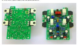
Jims audio is doing excellent job in PCB making without him I cannot have build NX amp.I like to build SX first I changed my mind because of the unavailability of SX PCB at that time.As price vs quality he done excellent job in PCB making.I support Jim's audio in my all future DIY builds.
I would like to thank Bonsai for providing such an excellent PCB from Jims Audio.
I would like to thank Bonsai for providing such an excellent PCB from Jims Audio.
Hey Bonsai,
Thanks for sharing this wonderful design for DIY 🙂
I have sourced the sx amp pcbs from jims audio and in the process of sourcing components..
Request help with clarifying my understanding of below
1. J2 should be shorted
2. R20 should be 2.2k 0.5W
3. Q3 should be BC547 through hole
4. R4 value is 15R on circuit diagram and 100k on pcb -- which one to go with? Is 0.5W critical for 100k resistor or any 0.25W would do?
5. Could not see C1 10uf, 50v on pcb (the smd pads on back side of pcb for this? )
Thanks
AndrewT, please keep comments about Jim's Audio off this thread.
You cannot go slinging accusations of theft etc without proof (and no, I don't want to see or hear what you have).
I have a mutual agreement with Jim's Audio to supply nx and sx PCB's and so far ther are about 100 or so happy customers.
Let's keep this thread about the amplifiers in question and leave the politics out of it.
Thank you
😎
Hello Balu,
1. J2 should be shorted - YES
2. R20 should be 2.2k 0.5W - YES. ADJUST R6 FOR MAXIMUM AND NOT MINIMUM AS IT STATES IN THE BUILD DOCUMENT
3. Q3 should be BC547 through hole - YES
4. R4 value is 15R on circuit diagram and 100k on pcb -- which one to go with? Is 0.5W critical for 100k resistor or any 0.25W would do? - 15 OHMS - BUT IT WILL BE SHORTED OUT VIA J2 ANYWAY. 0.25W IS OK
5. Could not see C1 10uf, 50v on pcb (the smd pads on back side of pcb for this? ) - YES - C1 IS 1206 SMD ON BACK OF PCB. THIS IS NOT CRITICAL - IF YOU CANNOT GET IT, LEAVE IT OFF. IT JUST FILTERS ANY REMAINING NOISE FROM THE OFFSET ADJUST CIRCUIT.
Good luck with your build!
Dear Andrew, I am currently using the V2.0.9 manual. I have found some discrepancies:
On page 52 PDTC143ET is printed on the bottom side of the PCB. However the BOM mentions PDTC144ET. I assume I have to use the PDTC144ET for U2 right?
On page 51 is no BC847 visible. Unfortunally my PCB's lack a printed silk screen at the bottom side. To be sure, am I correct that it has to be soldered where the yellow circle is? Also what value is the SMD component in the red circle?
Attachments


Dear Andrew, I am currently using the V2.0.9 manual. I have found some discrepancies:
On page 52 PDTC143ET is printed on the bottom side of the PCB. However the BOM mentions PDTC144ET. I assume I have to use the PDTC144ET for U2 right?
On page 51 is no BC847 visible. Unfortunally my PCB's lack a printed silk screen at the bottom side. To be sure, am I correct that it has to be soldered where the yellow circle is? Also what value is the SMD component in the red circle?
Hello Michael
1. U2 is PDTC144. This has internal 47k resistors (143 has 4.7k - too low)
2. If you look under where Q2 is (this is the NJW3281) you will see where the BC847 solders down. This is the sensing transistor for the Vbe compensation. Use tweezers and thin solder to place it.
3. Component in the red circle - sorry can you give me more info on your question?
Your boards are looking very good!
Last edited:
Bonzai,
the red circle in post1810 is just above the Vbe multiplier.
On the NX PCB that red circle is a 10uF ceramic capacitor.
the red circle in post1810 is just above the Vbe multiplier.
On the NX PCB that red circle is a 10uF ceramic capacitor.
ok - got it.
That is C3 - 10uF 25V 1206 MLCC capacitor. It decouples the bias spreader circuit (Q3 and Q20).
Michael, can you confirm that you have Version 2 PCB's?
(I have just got Microsoft Office again so will update the document shortly)
That is C3 - 10uF 25V 1206 MLCC capacitor. It decouples the bias spreader circuit (Q3 and Q20).
Michael, can you confirm that you have Version 2 PCB's?
(I have just got Microsoft Office again so will update the document shortly)
Hi Andrew and AndrewT,
Thanks Andrew, got it 🙂! Yes, I have version 2.0 (Nov 2014).
Thanks AndrewT, I have just added the 10 uF cap 🙂.
Thanks Andrew, got it 🙂! Yes, I have version 2.0 (Nov 2014).
Thanks AndrewT, I have just added the 10 uF cap 🙂.
Can someone explain what component goes at red circled pads of sx psu board?
https://goo.gl/photos/jF8RDaTkv1r7xZBE9
Thanks
https://goo.gl/photos/jF8RDaTkv1r7xZBE9
Thanks
Balu,
you can ignore it - its not used (I added it originally be able to take off 0V and V+ via a small 2 pin SIP connector).
you can ignore it - its not used (I added it originally be able to take off 0V and V+ via a small 2 pin SIP connector).
- Home
- Amplifiers
- Solid State
- SX-Amp and NX-Amp