Thanks ,waiting for this.Yes, I will post a circuit up tomorrow.
just before......fire!
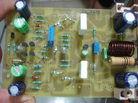
Poor man's sx-amplifier,or sx-ampl.with what i have😱
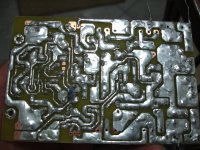
i will never use lead free solder again🙁
BTW it's on my plan testing this with one pair out biased in class A
Poor man's sx-amplifier,or sx-ampl.with what i have😱
i will never use lead free solder again🙁
BTW it's on my plan testing this with one pair out biased in class A
Attachments
Last edited:
Thanks pinnocchio.Nice job thimios! Hope you like the sound of it
Ciao!
Do
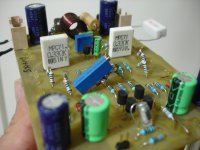
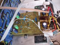
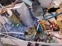
Here is the completed channel.
Attachments
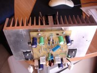
Thanks Bonsai ,i believe a small modification at the bias circuit is necessary .Very nice! I like the Sankens! They will work fine in this circuit.
It can't go down from 660mV from one emitter to other emitter(output transistors).
PS just now i see that the recommended current is 1.5A
Last edited:
Yes, I will post a circuit up tomorrow.
I will post it up later this week. Too busy at the moment!
Ok,never mind.I will post it up later this week. Too busy at the moment!
We can wait🙂
sx
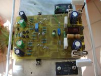
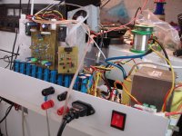
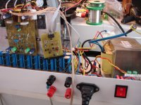
Today is a listening test day.
Power supply: +/-20V D.C
33000UF/Rail
EI transformer
Biased at 1.5A
One pair OUT.
Offset=0 mV absolutely stable.
From this first test it is clear,this is a very good sounding amplifier,deep bass,clear high .
Congratulations Bonsai good job!
PS measurement test some days later.
Thimios.
Last edited:
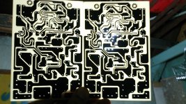
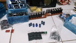
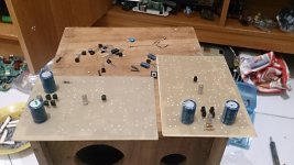
Good luck!🙂my first move. the poor boy sx boards

Here is the single sided sx-Amp (15 Watt Class A CFA) PCB layout in Gerber format I promised a few days ago.
I have not built this version (only the THP version)
So, please feel free to take a look.
The circuit is the same as for the one in the write-up on my website except that I have replaced C2 with a through hole electrolytic device and J2 is removed. Further, all the semiconductors are now through hole.
The overlay and circuit diagram are attached as .jpg
NOTE: THIS LAYOUT INCORPORATES THE UPDATED RESISTOR VALUES FOR R28, R29 AND R36 AND R37.
I don't know how to turn this into a .pdf file - anyone got any ideas? This will mean people can etch their own boards.
The write on this amplifier is on my website - here is a link for your convenience: Ovation sx-Amplifier: A 15 W class A Amplifier
Happy building!
hi mr bonsai. i get confuse about cap 2 10uf around tr 3.bc547. its different on single side and double layer schematic. why? regards
That's C2 - it simply decouples Q3 collector to emitter so that at HF its still a low impedance.
Q3 is the bias generator.
Note the sx-Amplifier bias generator doe not work like an ordinary Vbe multiplier - its actually measuring the voltage across the out devices emitter degen resistors and then controlling the base voltage across the output devices.
😎
Q3 is the bias generator.
Note the sx-Amplifier bias generator doe not work like an ordinary Vbe multiplier - its actually measuring the voltage across the out devices emitter degen resistors and then controlling the base voltage across the output devices.
😎
thanks mr bonsai for fast reply. so which schematic i must to built? , because on double layer schematic C2 its gone.thanks
Hmmm. How dis I miss that.
Please fit it per the single sided layout.
My DSTHP has the cap fitted. Il have to check the Gerbers - might be the circuit diagram that is missing it.
Please fit it per the single sided layout.
My DSTHP has the cap fitted. Il have to check the Gerbers - might be the circuit diagram that is missing it.
- Home
- Amplifiers
- Solid State
- SX-Amp and NX-Amp