This forum is about solid state amplifiers that the members construct and build.
One of the most important criteria for us is distortion. We dont care if you like it or not.
We are just hunting for a better solution. It can be fewer componets, higher speed, lower noise or lower distortion.
So please dont try to disturb our discussions.
One of the most important criteria for us is distortion. We dont care if you like it or not.
We are just hunting for a better solution. It can be fewer componets, higher speed, lower noise or lower distortion.
So please dont try to disturb our discussions.
When I am curious how it sounds, I build it. 😎It says nothing about how the amp sounds.
Or see rather Douglas Self books.51mA is too low for 0.22ohm emitter resistors. See my article on Class AB biasing.
Ed
25mV across Re is of course optimal bias. However, if you make extensive THD spectrum measurements on real world power amps, you will find little difference for 15-25mV bias (per one Re), thus 50mA per pair is fine. Going lower, high order harmonics start to rise to the level that is more than adequate.
If we look at an output with 1 pair of output transistors we often consider 21 mv over the emitter resistor as optimum.
With 0,22 ohm it is idle current 95 mA. If we parallel 2 pairs we can double the resistor and loose the same max output voltage.
Usually we take it little less because of a small loss in base stoppers. Lets say we choose 0,39 ohm. There we have the optimum current = 54 mA or for the 2 pairs 108 mA. Not considering the influence of the base stoppers.
With 4 pairs we can choose 0,68 ohm and have 31 mA in each pair to reach 124 mA total.
If we assume the output transistors to have a current gain of 100 the room for base stoppers is (2x0,22 - 0,39)x100/2 = 2,5 ohm
With 4 transistors (4x0,22 - 0,68) x100/4 = 5 ohm.
It seems like we can use paralleled output transistors without raising the idle current a lot and still have the same output voltage.
With so complicated amp the THD seems to be high.Circuit Evolution:
Actual THD is now 0.001674% at medium output level.
Vcc = Vee = 65V with four output pairs.
Application of some old technics to improve output beharvior.
Protection circuit trigger overload pin of UPC1237 integrated circuit.
I think to do two PCB - one to power output and other to VAS stage. I think to do other circuits topologies to define the best one to my ears.
You would expect it to be lower.
So much work for so little ....
... and why all the extra decimals ;-D 03111What's with chasing THD numbers? Is it an e-peen thing?
//
If we look at an output with 1 pair of output transistors we often consider 21 mv over the emitter resistor as optimum.
With 0,22 ohm it is idle current 95 mA. If we parallel 2 pairs we can double the resistor and loose the same max output voltage.
Usually we take it little less because of a small loss in base stoppers. Lets say we choose 0,39 ohm. There we have the optimum current = 54 mA or for the 2 pairs 108 mA. Not considering the influence of the base stoppers.
With 4 pairs we can choose 0,68 ohm and have 31 mA in each pair to reach 124 mA total.
If we assume the output transistors to have a current gain of 100 the room for base stoppers is (2x0,22 - 0,39)x100/2 = 2,5 ohm
With 4 transistors (4x0,22 - 0,68) x100/4 = 5 ohm.
It seems like we can use paralleled output transistors without raising the idle current a lot and still have the same output voltage.
Have you measured on real 2EF pairs or do you suggest based on simulations?
With 3 EF at the output i would have cascoded the VAS. And there is no reason to do something extra with the current generators as long as the input transistors are not cascoded.
With 3 pairs of output transistors there will of course be some components. So much work for so high output power...
With 3 pairs of output transistors there will of course be some components. So much work for so high output power...
Yes i have measured a lot of amplifiers. The 21 mv goes back to the first generation of stereo amplifiers with about 0,3% distortion in the 70:s.
When servicing amplifiers professionally i always measured the distortion and adjusted the bias current.
But I have checked it many times in the new millenium and it seems to fit. But of course different amplifier topologies can yield different answers.
With series connected Miller integrators i had lower bias current. But that could be that the distortion was so low anyway.
I have never simulated different idle currents because i dont get the same results as with real amplifiers.
I use simulators to check open loop gain and phase. But for that i need a simulated bias current. I check the simulator distortion but i have seen that it sometimes is far from the real amplifiers. I can not use the same transistor in several places in the amplifier but the simulator can.
Last edited:
The simulator also shows that 15mV is fine, but the lower voltage will be more affected by temperature.PMA said:25mV across Re is of course optimal bias. However, if you make extensive THD spectrum measurements on real world power amps, you will find little difference for 15-25mV bias (per one Re), thus 50mA per pair is fine. Going lower, high order harmonics start to rise to the level that is more than adequate.
This is true, but larger resistors and lower per-transistor currents will increase distortion. State-of-the-art amplifiers generally have 0.22 ohm emitter resistors and excellent thermal tracking.stigigemla said:With 0,22 ohm it is idle current 95 mA. If we parallel 2 pairs we can double the resistor and loose the same max output voltage.
I unfortunately don't have the equipment to measure distortion. The assumption that the output transistors are driven by a voltage source is accurate only for EF3 with the pre-driver and driver transistors operating in class A. EF2 or class AB drivers will be sensitive to Hfe differences between the NPN and PNP.stigigemla said:I have never simulated different idle currents because i dont get the same results as with real amplifiers.
Ed
Last edited:
You know Ed, there is a lot of myth spread through internet, based on simple simulations and incomplete analysis, that is not taking into account enough variables.The simulator also shows that 15mV is fine, but the lower voltage will be more affected by temperature.
I have just made for you, and others who might be interested, a set of measurements with a simple class AB amplifier, with MJL21193/4 single output pair, 0R22 Re resistors, and 4R7/200W load. The results with 8mV, 14mV and 21mV across one Re resistor are shown below.
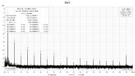
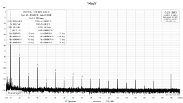
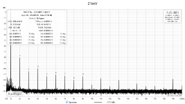
Please check them. This is my humble suggestion, not only to you, but to all simulation-only guys. NEVER give any strict suggestions based on simulations only. Just say maybe. You never know before you build the circuit. Go and build the circuit ad then optimise it (including idle current) to the best results you can get from the circuit. Then you may give suggestions, valid just for one circuit and existing implementation. Anything else is a stub. It is up to OP to show what his circuit can do, in a real world.
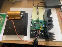
Last edited:
@PMA - Thanks for the measurements! A very apparent difference is that the measured data (of a real amplifier) shows both even and odd harmonics, while my simulation (of only a complementary emitter follower) shows only odd harmonics. The conclusion is the real amplifier has more distortion mechanisms than the one in my simulator.
I believe the simulator is quite accurate for what it does because bipolar transistors follow Ebers-Moll very closely. Inaccuracies are due to simplifying assumptions about the rest of the amplifier. I was very conscious of that and so I designed my amplifier in a way that the simplifying assumptions should hold true. I was doing hand analysis at the time. 😉
Ed
21mV over 8mV bias advantage can be seen at low power, as the output stage stays longer in class A, due to higher idle current. That's all.

THD vs. frequency keeps being reasonably flat.
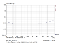
Sorry if I am OT, but I cannot stay silent when I read certain recommendations.
----------------
Now, 35 mV across 0R22 makes it even better

So, I am asking, where are the text-book suggestions on 21-25mV? We have known for years that it does not work.
THD vs. frequency keeps being reasonably flat.

Sorry if I am OT, but I cannot stay silent when I read certain recommendations.
----------------
Now, 35 mV across 0R22 makes it even better
So, I am asking, where are the text-book suggestions on 21-25mV? We have known for years that it does not work.
Last edited:
I think the distortion you are measuring is due to Hfe differences between NPNs and PNPs, variations in Hfe with Ic, and/or non-linearities in the VAS. These can far exceed the distortion due to the exponential current-voltage relationship.
Analyzing the causes of distortion is an intractable problem unless one makes simplifying assumptions (and designs the amplifier so that those assumptions hold true). I have now written special-purpose simulators for all of the blocks in my amplifier, and I think I have a good understanding of the distortion mechanisms. I can explain why simulators don't always produce the right answers.
Ed
Hi @PMA, could you share your schematic?
EF2/EF3 exhibits an optimal bias point and that's for sure. The mechanism is the non-linearity of the emitter output impedance combining with the fixed Re (such as 0.22 Ohm). There is a sweet point. Douglas Self verified that in his book.
Of course, it depends on what output level, usually I will take measurement at 5W, to get out of class A region.
I started a new thread, not to be OT here. There is the schematic as well.Hi @PMA, could you share your schematic?
Push-pull EF or 2EF output stage is probably the most frequently used output topology in class AB amplifiers. It is well covered in renowned design handbooks, like
Self, D.: Audio Amplifier Design Handbook (Newness)
or
Cordell, B.: Designing Audio Power Amplifiers (McGraw Hill)
Authors come to the conclusion that for the lowest distortion in class AB, voltage drop across an Re resistor (usually 0.1 to 0.47 ohm) should be about 22mV, as by Self below (he shows voltage between emitters, i.e. 2 x Re resistor):

Simulators (MicroCap, LTSpice) show +/- similar values. But how...
Self, D.: Audio Amplifier Design Handbook (Newness)
or
Cordell, B.: Designing Audio Power Amplifiers (McGraw Hill)
Authors come to the conclusion that for the lowest distortion in class AB, voltage drop across an Re resistor (usually 0.1 to 0.47 ohm) should be about 22mV, as by Self below (he shows voltage between emitters, i.e. 2 x Re resistor):
Simulators (MicroCap, LTSpice) show +/- similar values. But how...
- PMA
- Replies: 37
- Forum: Solid State
I am not so certain about smaller current in the output transistor and increasing distortion. Fast output transistors seem to work better on low currents with their low current amplification nearly constant. Of course - the capacitances is important too.
With the old 2N3055 or TIP:s it definitly was so.
You made me curious. The question if the VAS is a voltage or a current source has an answer. It depends on frequency, Miller compensation and gain. And of course the load.
I made a simulation of a very simple VAS with 47pF Miller capacitor and 0dB gain at 3MHz.
The output impedance was about 300kohm at DC sinking to 1 kohm at 400 kHz.
If we assume 2EF and that the transistors have a current gain of 100 the load at low frequencies would be about 8 x 100 x 100 = 80 kohm at DC.
With Ft about 50 MHz i assume 8 x 30 x 30 = 7,2k at 1 MHz. The VAS has probably lower output impedance at 1MHz than the input impedance of the output stage. These calculations are very uncertain so dont take the values as anything else as a very uncertain simulation.
But anyway i believe i can say that at high frequencies the VAS is more like a voltage source and at low frequencies more like a current source.
- Home
- Amplifiers
- Solid State
- Super Symmetrical Amplifier with THD = 0.003111% for 8 Ohms load