;-) With your help I got there on a BJT implementation. And then, not long after posting above but, of course, outside the 30 minute cutoff, I finally unblocked my feeble brain re a very basic Mosfet implementation.
Interestingly, one little "super regulator" I happen to own uses a TL071C op amp (driving a fet). Wouldn't GBW of 3Mhz be somewhat limiting?
Interestingly, one little "super regulator" I happen to own uses a TL071C op amp (driving a fet). Wouldn't GBW of 3Mhz be somewhat limiting?
Last edited:
Jan, you didn't grasp that the original circuit contains TWO feedback loops, one of them positive feedback. The proposed modification has a significant major benefit: it completely eliminates positive feedback. It also has a serendipitous, secondary result: at the same time it gets rid of positive feedback, it happens to ALSO attenuate input noise by >120 dB.
I chuckle that the proposed modification is defecated-upon by Walt Jung himself, (HERE). He fails to realize that the loop gain of the positive feedback loop is Av_opamp times the attenuation of the zener's lowpass filter. When you use a mans-man opamp instead of an AD825 (Av = 76dB), the positive feedback loop gain can be greater than 1. This is one under-appreciated reason why the AD797 (Av = 146 dB) doesn't work well in the Super Regulator. The LTC1150 (Av = 180 dB) would be even worse.
*Someone* does fail to understand the POS/NEG feedback setup in this regulator, and I don't think it is Jan Didden or Walt Jung.
That "Someone" fails to realize that the loop gain of the POS feedback loop is much, much less than the near unity gain of the NEG loop. From Vout to the OA (+) input there are *two* attenuations, one from the Vref bias resistor R4 against the diode Z of about 1 ohm (>70dB), and higher frequency attenuation of the R1-C7 filter. So, it should be obvious that the NEG feedback loop is heavily dominant when the reg is operating. The POS loop does come into play in the startup phase, and this is documented. See "Just how does it start?" for example.
Given these points, I would strongly suggest that feeding the reference diode from a complex current source setup is unnecessary and not advised.
The 71 will give lower performance - but whether you hear that depends on a zillion other factors. You might luck out 😉
I haven't really experimented with a FET as a pass device. The way I see it, the much lower gain/transconductance of a FET wrt a bipolar will result in lower measured performance. But it's worth a try if you feel like it.
jan
I haven't really experimented with a FET as a pass device. The way I see it, the much lower gain/transconductance of a FET wrt a bipolar will result in lower measured performance. But it's worth a try if you feel like it.
jan
Given these points, I would strongly suggest that feeding the reference diode from a complex current source setup is unnecessary and not advised.
Can't say I disagree Walt!
Hi Walt, thanks for your comments. I find that your first attenuation is 20*log10(4990/0.8) = 76 dB, and the second attenuation is 20*log10(100*2*pi*499*1.2E-4) = 32 dB at 100 Hz (the input ripple frequency), giving a total of 108 dB attenuation at 100 Hz. Multiplied by the opamp's open loop voltage gain at 100 Hz, the overall gain of the positive feedback loop can exceed 1 for some opamps (GBW > 25 MHz with high Avol) -- and those appear to be the cases that cause misery in simulation.From Vout to the OA (+) input there are *two* attenuations, one from the Vref bias resistor R4 against the diode Z of about 1 ohm (>70dB), and higher frequency attenuation of the R1-C7 filter. So, it should be obvious that the NEG feedback loop is heavily dominant when the reg is operating.
Does a JFET+zener diode qualify as a "complex current source" ?I would strongly suggest that feeding the reference diode from a complex current source setup is unnecessary and not advised.
Last edited:
1) Hi Walt, thanks for your comments. I find that your first attenuation is 20*log10(4990/0.8) = 76 dB, and the second attenuation is 20*log10(100*2*pi*499*1.2E-4) = 32 dB at 100 Hz (the input ripple frequency), giving a total of 108 dB attenuation at 100 Hz. Multiplied by the opamp's open loop voltage gain at 100 Hz, the overall gain of the positive feedback loop can exceed 1 for some opamps (GBW > 25 MHz with high Avol) -- and those appear to be the cases that cause misery in simulation.
2) Does a JFET+zener diode qualify as a "complex current source" ?
1) And, much more than 108dB at higher frequencies, where the RC filter is working, and OA gain is rolling off. Still not obvious here why all the paranoia. People have been building regulators like this for about 60 years. Myself, around 40 years or so.
FWIW, the problem with the 797 was at very HF, as Jan noted.
2) Compared to a single resistor, YES. That circuit of post #351 is much more complicated.
Last edited:
I haven't really experimented with a FET as a pass device. The way I see it, the much lower gain/transconductance of a FET wrt a bipolar will result in lower measured performance. But it's worth a try if you feel like it.
jan
I'm playing around with regulated supplies up to 12v which I would like to be 5A capable. I understand - correct me if I am wrong - the op amp would have to sink the full bjt bias current if the load wasn't drawing the full load. Can the AD825 do this? The fact that a mosfet pass device doesn't draw appreciable gate current is presumably an advantage in such a situation.
I'm playing around with regulated supplies up to 12v which I would like to be 5A capable. I understand - correct me if I am wrong - the op amp would have to sink the full bjt bias current if the load wasn't drawing the full load. Can the AD825 do this? The fact that a mosfet pass device doesn't draw appreciable gate current is presumably an advantage in such a situation.
Yes I agree with that reasoning. That a very good rationale to use a FET.
Jan
Hi Walt, you wrote
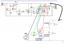
Whoops, there's been a misunderstanding. I've added the circuit of post #351, onto Jan's schematic of the Super Regulator, attached below. I hope it shows that only two components are new, the JFET and the 10V zener diode. The rest of the components are already present in the Super Regulator. I tried to call attention to this in the text of post #351, but apparently did not communicate it very well:2) Does a JFET+zener diode qualify as a "complex current source" ?
2) Compared to a single resistor, YES. That circuit of post #351 is much more complicated.
The new components are Pchannel Jfet J1, and zener diode D1. ... Components R1, R2, D2, and C1 on the attached LTSPICE schematic, exactly correspond to components R5, R4, D5, and C9 respectively, in the Super Regulator schematic.
Attachments
Hi Walt, you wrote
Whoops, there's been a misunderstanding. I've added the circuit of post #351, onto Jan's schematic of the Super Regulator, attached below. I hope it shows that only two components are new, the JFET and the 10V zener diode. The rest of the components are already present in the Super Regulator. I tried to call attention to this in the text of post #351, but apparently did not communicate it very well:
OK, that is more clear. But, why is it necessary at all? You haven't convinced me.
That said, if you wish to emulate an Isource to feed the ref diode, there are better ways, such as a N-Ch JFET pair cascoded, 2N5457 + 2n5459, etc. But, you will still need to screen the FETs and possibly tweak an R.
I can't help but wonder about all those hundreds (thousands?) of regulators out there using this type of topology, with this POS feedback "problem". Why haven't you warned us of it?
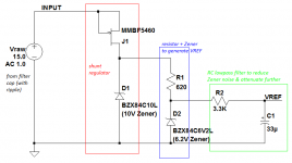
Hi Walt, the idea was to build a shunt regulator (JFET + 10V zener) to attenuate mains ripple, then use a conventional resistor+Zener to generate VREF, then filter it with an RC lowpass to reduce Zener noise and to attenuate ripple yet further. Not attempting to "feed the ref diode with an Isource"; instead I am feeding the shunt regulator (stage before the ref diode) with a single-component sloppy approximation of an Isource.
That isn't what your sch shows!
The title above says it all. One cannot reconcile the schematic inserting the double zener kludge into the ref path with the wordage above.
At this juncture I would just ask, what is your point with all of this? Have you ever built any of these regulators, such as the one you say is prone to startup problems? One that oscillates due to the use of the positive feedback path?
Hi Walt, the idea was to build a shunt regulator (JFET + 10V zener) to attenuate mains ripple, then use a conventional resistor+Zener to generate VREF, then filter it with an RC lowpass to reduce Zener noise and to attenuate ripple yet further. Not attempting to "feed the ref diode with an Isource"; instead I am feeding the shunt regulator (stage before the ref diode) with a single-component sloppy approximation of an Isource.
The title above says it all. One cannot reconcile the schematic inserting the double zener kludge into the ref path with the wordage above.
At this juncture I would just ask, what is your point with all of this? Have you ever built any of these regulators, such as the one you say is prone to startup problems? One that oscillates due to the use of the positive feedback path?
... the idea was to build a shunt regulator (JFET + 10V zener) to attenuate mains ripple, then use a conventional resistor+Zener to generate VREF, then filter it with an RC lowpass to reduce Zener noise and to attenuate ripple yet further.
Hi Walt, I've labeled the schematic (below) showing the shunt regulator, the resistor+Zener to generate VREF, and the RC lowpass filter.That isn't what your schematic shows. One cannot reconcile the schematic inserting the double zener kludge into the ref path with the wordage above.
The shunt regulator turns ripply +15V into less ripply (-52dB attenuated) +10V. The resistor+Zener generate +Vzener (about +6.2V in this case). The RC lowpass filter is single pole. What doesn't match up?
Yes I've built this regulator. I'm fooling around now with a new revision, that uses your VREF-derived-from-VOUT idea, along with an AD797 error amplifier. It's still early days and it's only in simulation, but I'm not liking the results I'm seeing in simulation. Thus far anyway, I prefer VREF-derived-from-VIN. The good news is, you can get quite delightfully huge attenuation from VIN to VREF, by adding a grand total of two additional components over and above the existing component count on the Super Regulator. The performance penalty of "paranoia" as you called it in post #366, is quite low. And so is the additional component cost.
Attachments
While I am a newbie tip-toeing around you giants and trying desperately to follow the discussion (Mark's last graphic is very helpful for me to follow along), Mark might be interested to know that Fidelity Audio's SPower HC regulators are advertised as having "a very low noise precision voltage reference which is fed via a filter circuit offering broadband filtration" and, from my observation of the PCB, it would seem it is driven from Vin rather than Vout. Of course, that doesn't suggest that it is the best approach and I do not have measurements of the regulator's performance.
Try a DN2540 cascode
The sch you showed before with the mirrored addon was connected to Vout, not Vin.
If you want a good clean feed for the reference diode, I don't think you can do better than a well-chosen FET cascode.
Take a close look at the *measured* performance data for the DN2540 pair in Fig. 2, where noise on Vin is down 150dB. How does the double-zener setup compare to that? Not in sims, but in actual operation.
Hi Walt, I've labeled the schematic (below) showing the shunt regulator, the resistor+Zener to generate VREF, and the RC lowpass filter.
The shunt regulator turns ripply +15V into less ripply (-52dB attenuated) +10V. The resistor+Zener generate +Vzener (about +6.2V in this case). The RC lowpass filter is single pole. What doesn't match up?
Yes I've built this regulator. I'm fooling around now with a new revision, that uses your VREF-derived-from-VOUT idea, along with an AD797 error amplifier. It's still early days and it's only in simulation, but I'm not liking the results I'm seeing in simulation. Thus far anyway, I prefer VREF-derived-from-VIN. The good news is, you can get quite delightfully huge attenuation from VIN to VREF, by adding a grand total of two additional components over and above the existing component count on the Super Regulator. The performance penalty of "paranoia" as you called it in post #366, is quite low. And so is the additional component cost.
The sch you showed before with the mirrored addon was connected to Vout, not Vin.
If you want a good clean feed for the reference diode, I don't think you can do better than a well-chosen FET cascode.
Take a close look at the *measured* performance data for the DN2540 pair in Fig. 2, where noise on Vin is down 150dB. How does the double-zener setup compare to that? Not in sims, but in actual operation.
Hi Walt, sorry that the drawing in post #369 misled you. It was merely intended to show that four components of the Super Regulator are reused, and the total number of new components is 2. The Thick Black Line denotes which nodes are the raw input to the VREF generator. Perhaps I should have used arrowheads instead of dots at the ends of this line. Sorry for the confusion.The sch you showed before with the mirrored addon was connected to Vout, not Vin.
I agree that it is possible (in fact straightforward) to build a much much better current source than a single 2N5460 / MMBT5460 with gate tied to source. With a really great current source, one can get even better attenuation of Vin@100Hz than the -122dB shown here. (It should not be difficult: in simulation the 2N5460's rds was only 10k! yuck!) But I find it delightfully compact to add only two new parts to the Super Regulator's part-count, and get a VREF where volts of input ripple become microvolts of VREF ripple - with attenuation getting larger and larger at higher frequencies.
I agree, if someone thinks they need more than -122dB, there are straightforward ways to achieve it. For example: once you've got a truly great current source, you might think about abandoning the shunt regulator stage entirely. But I think the new circuit won't have quite the excellent bang-for-the-buck performance/cost ratio, as (NewParts=2, Attenuation=-122dB).
Thanks again for your comments.
Mark Johnson
When I did the regulator bake-off, my supposition was that Zout would correlate (inversely) with the listening panel's impression. There's still a lot of dust in the data, but low frequency PSRR instead seemed more important, although you wouldn't head to the pari-mutuel window with the results.
As I've mentioned before, if you modulate the supply rail and look at the artifacts via FFT you soon realize that the good sounding regulators (Jung-Didden, Sjostrom) leave a very light footprint, and others which are low Z, great PSRR and low noise are disappointing. The guess that this might be true was provided by a fellow DIYr who followed up the article with a letter to Jan.
As I've mentioned before, if you modulate the supply rail and look at the artifacts via FFT you soon realize that the good sounding regulators (Jung-Didden, Sjostrom) leave a very light footprint, and others which are low Z, great PSRR and low noise are disappointing. The guess that this might be true was provided by a fellow DIYr who followed up the article with a letter to Jan.
WJ edited out most of the obfuscating wordage..
Thanks again for your comments.
Mark Johnson
Oh, I am noting here you simply flat out ignored most of what I said in post 375.
If you want a good clean feed for the reference diode, I don't think you can do better than a well-chosen FET cascode.
Take a close look at the *measured* performance data for the DN2540 pair in Fig. 2, where noise on Vin is down 150dB. How does the double-zener setup compare to that? Not in sims, but in actual operation.
__________________
And, is the -122dB you quoted real data, or another sim?
Last edited:
Hi Walt, congratulations on your measured performance of -150dB using the bias multiplier cascode. Your suspicions are correct, I have never measured an attenuation that deep. Your further suspicions are correct, I have never built the exact DN2540N5 circuits you show in Audio Express 4/09 page 40. It is unlikely that I will; applying that circuit to create a low-ripple VREF for a voltage regulator, strikes me as a lot of extra complexity to get those final 30 dB of attenuation.
To my tastes, it seems preferable and easier to get those final 30dB by making a couple of tiny tweaks: Switch from a 25 ohm dynamic impedance zener, to an 0.8 ohm dynamic impedance LM329 IC (zero additional parts, gives 29dB more atten), and also switch from an 2N5460/MMBF5460 with no source resistor (rds=10K), to an LSK389 with source resistor (rout=30K). One additional part, gives 9dB more attenuation. Your further suspicions are correct, -122dB is from hand calculation rather than measurement. Simulation happens to agree with hand calculation in this case. The regulator I did build & measure, did not have a JFET in the shunt regulator, just a resistor. I didn't bother to measure its ripple attenuation on VREF quantitatively, beyond the qualititative observation that "I can't see any ripple on VREF at the scope's lowest mV/div setting". It wasn't important to me, to build instrumentation that measured the exact number of microvolts / nanovolts of ripple I was getting on VREF. I'm happy to assume that a reasonable PCB layout will give results reasonably close to the hand calculations. Spot-check with scope, done.
Or, it may be appropriate to wonder: how much ripple attenuation on VREF is enough? Maybe 120 dB suffices (1V ripple on Vin produces 1uV ripple on Vout). Maybe 100dB suffices. Why kill a fly with a bazooka? It's still dead if you merely kill it with a swatter.
Thanks again for your comments,
Mark Johnson
Last edited:
Post 358
Post 370
I'm glad we have violent agreement on how to get a good Vref when driven by Vin and we can split hairs over whether the cost of a few extra parts is worth it. 😀
Presumably in a MOSFET pass device setup rather than BJT setting Vref from Vin becomes a necessity? I also seem to be tying myself in knots as to how to power the op-amp in this situation. Again, is one forced to power from Vin? How important is a stable supply for the op amp?
Yes the JFET and the 10V zener diode form a shunt (pre)regulator which adds another ~ 52 dB of attenuation, no matter what input you drive it with. ...... You could attenuate even more, another 15-20 dB, if you used an active zener with a lower dynamic resistance (TL431). But that would be a negative feedback minor loop contained within a positive feedback major loop: bleah! Far more preferable / safer to increase the dynamic resistance of the current source via cascoding. But that would dilute the excellent bang-for-the-buck (2 cheap parts / 52 dB attenuation) you get with the JFET + zener.
Post 370
.... there are better ways, such as a N-Ch JFET pair cascoded, 2N5457 + 2n5459, etc. But, you will still need to screen the FETs and possibly tweak an R.
I'm glad we have violent agreement on how to get a good Vref when driven by Vin and we can split hairs over whether the cost of a few extra parts is worth it. 😀
Presumably in a MOSFET pass device setup rather than BJT setting Vref from Vin becomes a necessity? I also seem to be tying myself in knots as to how to power the op-amp in this situation. Again, is one forced to power from Vin? How important is a stable supply for the op amp?
- Home
- The diyAudio Store
- Super Regulator