Teddy considers the first stage to be a voltage regulator
Do you agree to that Mark?
Teddy considers the first stage [of the SuperTeddy circuit] to be a voltage regulator
I guess Wikipedia agrees to that. Here is a figure I copied from the Wikipedia article titled Voltage Regulator
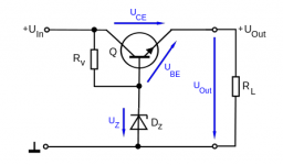
Wikipedia shows a (rudimentary) reference voltage generator, consisting of resistor Rv and Zener diode Dz, supplying a constant voltage to the input of follower Q. The follower's output is the regulated voltage. The Wikipedia circuit has the same basic elements as the first half of the SuperTeddy circuit, and the elements are connected together the same way. So if Wikipedia calls one of them a Voltage Regulator, I guess they have to call the other one a Voltage Regulator, as well.
Wikipedia says A voltage regulator is designed to automatically maintain a constant voltage level. A voltage regulator may be a simple "feed-forward" design or may include negative feedback control loops. It may use an electromechanical mechanism, or electronic components. Depending on the design, it may be used to regulate one or more AC or DC voltages.
If you take that as your definition, your pattern-to-be-matched, then I think the first half of the SuperTeddy circuit is an exact match which fits the definition quite well. On the other hand, if you prefer a different definition of "Voltage Regulator," that definition might possibly exclude the SuperTeddy.
Do you agree to that Mark?
I guess Wikipedia agrees to that. Here is a figure I copied from the Wikipedia article titled Voltage Regulator
Wikipedia shows a (rudimentary) reference voltage generator, consisting of resistor Rv and Zener diode Dz, supplying a constant voltage to the input of follower Q. The follower's output is the regulated voltage. The Wikipedia circuit has the same basic elements as the first half of the SuperTeddy circuit, and the elements are connected together the same way. So if Wikipedia calls one of them a Voltage Regulator, I guess they have to call the other one a Voltage Regulator, as well.
Wikipedia says A voltage regulator is designed to automatically maintain a constant voltage level. A voltage regulator may be a simple "feed-forward" design or may include negative feedback control loops. It may use an electromechanical mechanism, or electronic components. Depending on the design, it may be used to regulate one or more AC or DC voltages.
If you take that as your definition, your pattern-to-be-matched, then I think the first half of the SuperTeddy circuit is an exact match which fits the definition quite well. On the other hand, if you prefer a different definition of "Voltage Regulator," that definition might possibly exclude the SuperTeddy.
Attachments
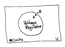
Jan, I think that's quite an interesting topic! If we divide the universe U of all possible circuits, into two sets: (i) the set of all Voltage Regulator circuits; and (ii) the set of all circuits which are NOT Voltage Regulators, we get the attached Venn Diagram.
And this suggests a fascinating question: Of all Voltage Regulator circuits, which one is closest to the borderline? Which Voltage Regulator circuit meets the membership requirements with the least excess? Suppose that is circuit "A" on the Venn Diagram. It is the worst possible Voltage Regulator that is still a voltage regulator.
The converse question is fascinating too: of all NOT Voltage Regulator circuits, which one is closest to the borderline? Which NOT Voltage Regulator circuit just barely misses the membership requirements by the smallest deficiency? Suppose that is circuit "B" on the Venn Diagram. It is the best possible NOT Voltage Regulator that is still not a voltage regulator.
Can we interpolate between A and B? Can we invent a continuum of circuits that stretches from A to B, allowing us to get even closer to the borderline (on either side)? Can we find a circuit that is exactly ON the borderline?
I suspect that we can. I have drawn up three possible continuums of circuits; they are attached below.
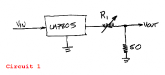
The schematic labeled "Circuit 1" most certainly is a voltage regulator when we set R1 = 1 microohm. Circuit 1 most certainly is NOT a voltage regulator when we set R1 = 10 megohms. But what about in-between? What setting of R1 produces point "A" in the Venn Diagram, a circuit that is in the set of Voltage Regulators, but just barely? What setting produces point "B"? Can we tell, just by inspecting the schematic, whether the point "A" circuit1 is, or is not, a Voltage Regulator?
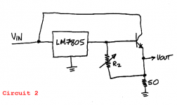
The schematic labeled "Circuit 2" most certainly is a voltage regulator when we set R2 = 1 microohm. (This shorts out the NPN, making it irrelevant). Some people might argue that Circuit 2 is NOT a voltage regulator when we set R2 = 10 megohms, because it has below-average Load Regulation. But what about R2 values in-between? When we set R2 to produce point "A" in the Venn Diagram, can we tell, just by inspecting the schematic, whether the point "A" circuit2 is, or is not, a Voltage Regulator?
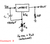
The schematic labeled "Circuit 3" most certainly is a voltage regulator when we set R3 = 1 nanoohm. Circuit 2 is NOT a voltage regulator when we set R3 = 7 ohms, because it has no Line Regulation whatsoever, at 60 Hz. But what about R3 values in-between? When we set R3 to produce point "A" in the Venn Diagram, can we tell, just by inspecting the schematic, whether the point "A" circuit3 is, or is not, a Voltage Regulator?
Thank you for suggesting a thought provoking line of inquiry, Jan! It was pleasant to think about the ideas.
And this suggests a fascinating question: Of all Voltage Regulator circuits, which one is closest to the borderline? Which Voltage Regulator circuit meets the membership requirements with the least excess? Suppose that is circuit "A" on the Venn Diagram. It is the worst possible Voltage Regulator that is still a voltage regulator.
The converse question is fascinating too: of all NOT Voltage Regulator circuits, which one is closest to the borderline? Which NOT Voltage Regulator circuit just barely misses the membership requirements by the smallest deficiency? Suppose that is circuit "B" on the Venn Diagram. It is the best possible NOT Voltage Regulator that is still not a voltage regulator.
Can we interpolate between A and B? Can we invent a continuum of circuits that stretches from A to B, allowing us to get even closer to the borderline (on either side)? Can we find a circuit that is exactly ON the borderline?
I suspect that we can. I have drawn up three possible continuums of circuits; they are attached below.
The schematic labeled "Circuit 1" most certainly is a voltage regulator when we set R1 = 1 microohm. Circuit 1 most certainly is NOT a voltage regulator when we set R1 = 10 megohms. But what about in-between? What setting of R1 produces point "A" in the Venn Diagram, a circuit that is in the set of Voltage Regulators, but just barely? What setting produces point "B"? Can we tell, just by inspecting the schematic, whether the point "A" circuit1 is, or is not, a Voltage Regulator?
The schematic labeled "Circuit 2" most certainly is a voltage regulator when we set R2 = 1 microohm. (This shorts out the NPN, making it irrelevant). Some people might argue that Circuit 2 is NOT a voltage regulator when we set R2 = 10 megohms, because it has below-average Load Regulation. But what about R2 values in-between? When we set R2 to produce point "A" in the Venn Diagram, can we tell, just by inspecting the schematic, whether the point "A" circuit2 is, or is not, a Voltage Regulator?
The schematic labeled "Circuit 3" most certainly is a voltage regulator when we set R3 = 1 nanoohm. Circuit 2 is NOT a voltage regulator when we set R3 = 7 ohms, because it has no Line Regulation whatsoever, at 60 Hz. But what about R3 values in-between? When we set R3 to produce point "A" in the Venn Diagram, can we tell, just by inspecting the schematic, whether the point "A" circuit3 is, or is not, a Voltage Regulator?
Thank you for suggesting a thought provoking line of inquiry, Jan! It was pleasant to think about the ideas.
Attachments
Jan, I think that's quite an interesting topic! If we divide the universe U of all possible circuits, into two sets: (i) the set of all Voltage Regulator circuits; and (ii) the set of all circuits which are NOT Voltage Regulators, we get the attached Venn Diagram.
And this suggests a fascinating question: Of all Voltage Regulator circuits, which one is closest to the borderline? Which Voltage Regulator circuit meets the membership requirements with the least excess? Suppose that is circuit "A" on the Venn Diagram. It is the worst possible Voltage Regulator that is still a voltage regulator.
The converse question is fascinating too: of all NOT Voltage Regulator circuits, which one is closest to the borderline? Which NOT Voltage Regulator circuit just barely misses the membership requirements by the smallest deficiency? Suppose that is circuit "B" on the Venn Diagram. It is the best possible NOT Voltage Regulator that is still not a voltage regulator.
Can we interpolate between A and B? Can we invent a continuum of circuits that stretches from A to B, allowing us to get even closer to the borderline (on either side)? Can we find a circuit that is exactly ON the borderline?
I suspect that we can. I have drawn up three possible continuums of circuits; they are attached below.
The schematic labeled "Circuit 1" most certainly is a voltage regulator when we set R1 = 1 microohm. Circuit 1 most certainly is NOT a voltage regulator when we set R1 = 10 megohms. But what about in-between? What setting of R1 produces point "A" in the Venn Diagram, a circuit that is in the set of Voltage Regulators, but just barely? What setting produces point "B"? Can we tell, just by inspecting the schematic, whether the point "A" circuit1 is, or is not, a Voltage Regulator?
The schematic labeled "Circuit 2" most certainly is a voltage regulator when we set R2 = 1 microohm. (This shorts out the NPN, making it irrelevant). Some people might argue that Circuit 2 is NOT a voltage regulator when we set R2 = 10 megohms, because it has below-average Load Regulation. But what about R2 values in-between? When we set R2 to produce point "A" in the Venn Diagram, can we tell, just by inspecting the schematic, whether the point "A" circuit2 is, or is not, a Voltage Regulator?
The schematic labeled "Circuit 3" most certainly is a voltage regulator when we set R3 = 1 nanoohm. Circuit 2 is NOT a voltage regulator when we set R3 = 7 ohms, because it has no Line Regulation whatsoever, at 60 Hz. But what about R3 values in-between? When we set R3 to produce point "A" in the Venn Diagram, can we tell, just by inspecting the schematic, whether the point "A" circuit3 is, or is not, a Voltage Regulator?
Thank you for suggesting a thought provoking line of inquiry, Jan! It was pleasant to think about the ideas.
You worry too much. If it uses feedback to 'regulate' the output, it regulates. If not, then not. There, saved you a lot of agony. Now go fix that wikipedia page 🙂
Jan

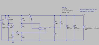
Firstly, if it isn't appropriate to continue to explore a high quality, high current Mosfet series pass regulator here please let me know and I will start another thread in the power supplies section of the forum. It would be good, however, to have the participants here contributing there.
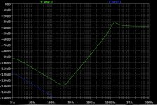
Here's a simple reg circuit. Nothing original here from me. Vref and Vs for op amp from Vin. Mark's circuit for Vref. I explored using the LTC1150 as the op amp but it oscillated with a step in load so this uses a cheap 30p part instead. Performance is, I guess, good but not nearly as good as the Jung/Didden regulator out past 1kHz.
How to improve from here:
1. Better current source for the Vref zener?
I tried, unsuccessfully, to apply some of the guidance from "The Art of Electronics", namely bipolar transistors make better current sources than JFETs. I haven't yet tried the cascode suggestion. (BTW it was odd, to me at least, that with the LTC1150 as the op amp, the noise rejection of the Vref circuit flattened at -160dB rather than continuing to decline.)
2. Vref from Vout?
The use of a MFET for the pass device would seem to make this rather challenging. And then there's Mark's warning with respect to compounding negative and positive feedback circuits. Much to be gained here?
3. A different op amp?
As Mark might say, use a "man's" op amp? This cheap'o op amp has a GBW of just 3MHz and CMRR and PSRR of 100dB. It benefits from a low pass filter to its supply (whereas the LTC1150 did not). I'm still struggling with my attempts to drop a AD797A or AD825 into the circuit but will try to get that nut cracked today.
4. Run the op amp supply from Vout?
As with 2, this would seem challenging. In a different thread Mark had suggested a circuit which allowed the op amp to start with Vin and switch to Vout when it was up and running. I tried this with the LTC1150 and couldn't get it to work. I'll try again with this op amp.
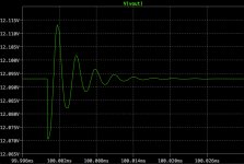
5. Dampen the transient response?
Mark will perhaps highlight that Vout's reaction to a very large kick in load looks like an underdamped control system. I will have to get out my notes and figure out implied zeta and phase margin. But how to manage this in this sort of circuit?
6. Implement Kelvin sense capability
7. Other?
cheers
Steve
Here's a simple reg circuit. Nothing original here from me. Vref and Vs for op amp from Vin. Mark's circuit for Vref. I explored using the LTC1150 as the op amp but it oscillated with a step in load so this uses a cheap 30p part instead. Performance is, I guess, good but not nearly as good as the Jung/Didden regulator out past 1kHz.
How to improve from here:
1. Better current source for the Vref zener?
I tried, unsuccessfully, to apply some of the guidance from "The Art of Electronics", namely bipolar transistors make better current sources than JFETs. I haven't yet tried the cascode suggestion. (BTW it was odd, to me at least, that with the LTC1150 as the op amp, the noise rejection of the Vref circuit flattened at -160dB rather than continuing to decline.)
2. Vref from Vout?
The use of a MFET for the pass device would seem to make this rather challenging. And then there's Mark's warning with respect to compounding negative and positive feedback circuits. Much to be gained here?
3. A different op amp?
As Mark might say, use a "man's" op amp? This cheap'o op amp has a GBW of just 3MHz and CMRR and PSRR of 100dB. It benefits from a low pass filter to its supply (whereas the LTC1150 did not). I'm still struggling with my attempts to drop a AD797A or AD825 into the circuit but will try to get that nut cracked today.
4. Run the op amp supply from Vout?
As with 2, this would seem challenging. In a different thread Mark had suggested a circuit which allowed the op amp to start with Vin and switch to Vout when it was up and running. I tried this with the LTC1150 and couldn't get it to work. I'll try again with this op amp.
5. Dampen the transient response?
Mark will perhaps highlight that Vout's reaction to a very large kick in load looks like an underdamped control system. I will have to get out my notes and figure out implied zeta and phase margin. But how to manage this in this sort of circuit?
6. Implement Kelvin sense capability
7. Other?
cheers
Steve
Attachments
U1 sees different DC resistances on it's inputs.
-IN sees 740||1k||120uF
+IN sees 3k3||470uF
This will lead to an increased tempco as well as an output offset.
The tempco will change the offset.
-IN sees 740||1k||120uF
+IN sees 3k3||470uF
This will lead to an increased tempco as well as an output offset.
The tempco will change the offset.
No, but the input pair expect to run at the same current.
It is implied in the opamp datasheet where they tell us about applying an offset correction to the 3 pins of a single opamp.
They state explicitly that the tempco is worse if offset is adjust at these pins.
Setting the offset in error by deliberately mis-terminating the input pins has a very similar effect to applying an offset correction.
W.Jung and the other opamp designers who are Members here will have real data on this effect.
I remember your original article set the input resistances to be equal. You must have had an inkling to the same problem, else you would not have added the matching resistor.
Last edited:
No, but the input pair expect to run at the same current.
It is implied in the opamp datasheet where they tell us about applying an offset correction to the 3 pins of a single opamp.
They state explicitly that the tempco is worse if offset is adjust at these pins.
Setting the offset in error by deliberately mis-terminating the input pins has a very similar effect to applying an offset correction.
W.Jung and the other opamp designers who are Members here will have real data on this effect.
I remember your original article set the input resistances to be equal. You must have had an inkling to the same problem, else you would not have added the matching resistor.
Don't bother to agree with me, I've already changed my mind 😎
The thing is that all these effects are affected by the loopgain.
For instance if your input mismatch impedance is 1k, and the input bias offset current is say 500nA, your input offset voltage will be a whopping 500uV.
But since the closed loop gain is something like x 2, it will not be more than a mV or so.
The tempco stuff will be similar.
You don't really expect me to learn nothing in 20 years do you? 😉
Jan
I'm amazed that Belleson has got a patent for using a JFET + BJT. US 2010/0327834 A1
Whoops, that's not the correct citation. That's only the patent application. HERE is the actual issued patent: 8,294,440.
What is patented is the simultaneous use of 3 circuit features: (JFET+BJT); (Vref diode not driven by input); (Opamp positive supply = output AND opamp negative supply NOT ground). It's not merely (JFET + BJT). By the way, the Audio Express magazine version of the Jung Super Regulator (pub. 2000) is cited as prior art: Figure 2.
SGK, take a look at posts #36 & 37 in this thread. Jan Didden feels that external diodes across the opamp inputs are good practice. Even if the opamp is has FET inputs (like your LTC1150) and can tolerate a deltaV of 20 volts. I imagine he feels these diodes are extra double specially good when one of the opamp's inputs is biased from Vunregulated and the other is biased from Vregulated.
I think it would be beneficial to re-read chapter 4 of Bob Cordell's book, paying special attention to sections 4.5-4.7. This is where he shows how to simulate the open loop frequency response of a negative feedback control system, and how to interpret the results.
I think it would be beneficial to re-read chapter 4 of Bob Cordell's book, paying special attention to sections 4.5-4.7. This is where he shows how to simulate the open loop frequency response of a negative feedback control system, and how to interpret the results.
SGK, take a look at posts #36 & 37 in this thread. Jan Didden feels that external diodes across the opamp inputs are good practice. Even if the opamp is has FET inputs (like your LTC1150) and can tolerate a deltaV of 20 volts. I imagine he feels these diodes are extra double specially good when one of the opamp's inputs is biased from Vunregulated and the other is biased from Vregulated.
Ok I had read that and another discussion that the diodes weren't needed for the AD797A but were recommended for the AD825. Plus they aren't in a reg circuit I have which uses this op amp. However, it seems they're advisable in any case as "good practice".
I think it would be beneficial to re-read chapter 4 of Bob Cordell's book, paying special attention to sections 4.5-4.7. This is where he shows how to simulate the open loop frequency response of a negative feedback control system, and how to interpret the results.
Thanks I will take a look. I haven't gotten as far as checking loop gain and phase margin. I was just trying to relate our earlier discussion from here to the output I observed.
PS: for now I couldn't get the LTC1150 to withstand any sort of step in load and so for now I am modelling with the TL071
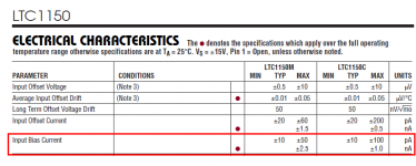
In a chopper stabilized opamp like the LTC1150 that SGK is using?U1 sees different DC resistances on it's inputs.
-IN sees 740||1k||120uF
+IN sees 3k3||470uF
This will lead to an increased tempco as well as an output offset.
The tempco will change the offset.
Rthev_neg = 425
Rthev_pos = 3300
Voffset = Ibias * (Rp - Rn) = 2.9 microvolts
Attachments
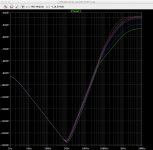
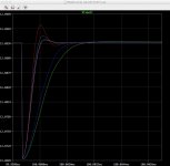
I just realised I had the wrong transistor in my previous output charts. It's also interesting to compare the noise regulation of that circuit with different transistors, observing that the one which produces the best noise rejection doesn't have the best transient response (Iload kicked from 0.25A to 5A). Here's some new charts.
Lots more work to do...
Lots more work to do...
Attachments
Ok I had read that and another discussion that the diodes weren't needed for the AD797A but were recommended for the AD825. Plus they aren't in a reg circuit I have which uses this op amp. However, it seems they're advisable in any case as "good practice".
Lots of people do opamp rolling, mixing and matching diverse types and changing from bjt to jfet input opamps at will 🙂
So in that sense it can be considered a precaution.
But you're absolutely right, if you know what you are doing you don't need them always.
jan
You worry too much. If it uses feedback to 'regulate' the output, it regulates. If not, then not. There, saved you a lot of agony. Now go fix that wikipedia page 🙂
Jan
Amen.
- Home
- The diyAudio Store
- Super Regulator