G’day.
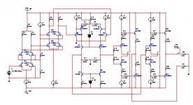
Attached below is a preliminary simulation of a fully differential preamplifier I’ve designed to give 100mVrms sensitivity to the 512+512W rms class A power amplifier I’m building.
The input stage is comprised of two cascaded, cascoded differential amplifiers using precision matched U404 JFETs running low drain load resistance (2k) to keep the bandwidth high and relatively high tail currents (5mA), to keep gm high so as to get a decent amount of voltage gain out of each stage.
An emitter follower buffered and cascoded differential VAS follows. Although not simulated yet, the common mode output voltage of the VAS outputs will be steered to 0V with a servo (as is necessary with the differential op-amp topology). For simulation purposes, I just tweaked the value of the VAS current sink bias battery to get the common mode voltage to 0V. The differential VAS is heavily emitter-degenerated for the best linearity and a pair of “diamond buffers” form the complementary output stages.
Simulation results so far look promising:
Single ended open loop gain is 72.9dB with the –3dB roll off point at 1.2MHz.
Open loop THD driving 8Vp-p (approx 2mVp-p single ended input) into 1000 ohms at 20kHz is just 0.034%
This thing is going to run with a closed loop gain of about 20.
I think I’ve pretty much optimised the design the best I can for the lowest THD. Before finalising the design and starting to layout the PCB I just though I’d just post the design here to see if anyone out there spot any obvious improvements.
Cheers,
Glen
Attachments
Interesting G.Klein 🙂
I know you are good with transistors (from suzyj guitar preamp topic)
Could you just attach a bit bigger image.
Then I am sure several will be able to tell,
what they think is good or less good.
Regards
lineup
I know you are good with transistors (from suzyj guitar preamp topic)
Could you just attach a bit bigger image.
Then I am sure several will be able to tell,
what they think is good or less good.
Regards
lineup
OK, here it is. With differential feedback applied and the common mode voltage servo added.
One thing I should have mentioned in the first post is that I’m using a differential preamplifier because my power amplifier is bridged design, which has differential inputs. Also note that this is a single ended input to differential output design. Due to the differential feedback, it necessarily has low input impedance (2k).
This preamp is to be preceded with a discrete fet input voltage follower configured op-amp to give high input impedance.
Cheers,
Glen
One thing I should have mentioned in the first post is that I’m using a differential preamplifier because my power amplifier is bridged design, which has differential inputs. Also note that this is a single ended input to differential output design. Due to the differential feedback, it necessarily has low input impedance (2k).
This preamp is to be preceded with a discrete fet input voltage follower configured op-amp to give high input impedance.
An externally hosted image should be here but it was not working when we last tested it.
Cheers,
Glen
My opinion is that such design is way too complex for me to even be able to look at the schematic and grasp what it should do. You are using 25 transistor, and still don´t have the current sources "unpacked", and there are many of them...
I wonder who would design a PCB for this
I wonder who would design a PCB for this

Man, if you`re not joking then you must be crazy😀
Do you have the extra room for that amp?
The idea with the freezer is also very good!
Why all that electronics for a preamp??
SENSIBLE MINIMALISM IS THE WAY TO GO!
Do you have the extra room for that amp?
The idea with the freezer is also very good!
Why all that electronics for a preamp??
SENSIBLE MINIMALISM IS THE WAY TO GO!
To screw a bulb into a socket old engineers take a stool, stand on it, and screw the bulb into the socket.
Young engineer needs additionally a team of 8 younger engineers to do the job: 4 to rotate the stool, 4 to go around to prevent dizziness.
Computer. 😉
Young engineer needs additionally a team of 8 younger engineers to do the job: 4 to rotate the stool, 4 to go around to prevent dizziness.
kubeek said:
I wonder who would design a PCB for this
Computer. 😉
I am not talking about money.Upupa Epops said:Twony five transistors cost cca up to one Euro and it isn´t " big money ", Kubeek.... 😀
In DIY, someone has to make the boards, solder the components and with 25 transistors a chance of some error is much higher than with less devices. Don´t forget that with increasing nuber of active devices, there are also more passives, traces and joints.
I understand that for production of huge series made by machines it is not a problem, but I do not want to complicate my life by using a preamp which in this case will have a very high chance of failure because of its complexity.
Show me a program which will take this schematic and produce a more than good board, while taking in account all rules and tinkering you would do when you design board for a superb amp or preamp.Wavebourn said:
Computer. 😉
There has to be someone who sits few hours or days by the computer and plays with the design.
And a freezer won´t help, the heat extracted from inside is produced on the rear side of the freezer through the cooling fins.
G.Kleinschmidt, you live in Australia, I guess it is not cold there like on the south pole?
1024W in class A, that´s something like 3-4kW heat, isn´t?
You would have to have a) heatsink on the wall of the house sized like 1x1m
b) Really big and efficient air-conditioner.
Both possibilites are expensive and are not worth the trouble.
Your argument is funny....if you are not able correctly solder cca one hundred devices, make rather something else.... 😎
I know you've said this in fun, but some parts of Australia have weather like in Britain or Canada.kubeek said:G.Kleinschmidt, you live in Australia, I guess it is not cold there like on the south pole?
In fact my problem isn´t soldering, but making the board. You know, when you draw all the traces by a pen and etch the board, the results aren´t satisfying.
I am trying to make the toner transfer method working, but don´t have luck with paper. Or maybe my copymachine is the problem.
Anyway, let´s get back to the initial topic...
I am trying to make the toner transfer method working, but don´t have luck with paper. Or maybe my copymachine is the problem.
Anyway, let´s get back to the initial topic...
lndm said:
I know you've said this in fun, but some parts of Australia have weather like in Britain or Canada.
I live with weather like in Britain or Canda, but still I would switch on something that produces such amount of heat only in winter.
My computer consumes something like 400W, and in summer I have to switch it off like an hour before I go to sleep because of the heat it makes.
kubeek said:
I live with weather like in Britain or Canda, but still I would switch on something that produces such amount of heat only in winter.
My computer consumes something like 400W, and in summer I have to switch it off like an hour before I go to sleep because of the heat it makes.
I currently use the amp that consumes 1300W. More power would cause powering problems.
*Groan*
1) My Class A design uses a low voltage power supply for the Class A stages which are driven by class A/B stages to track the output voltage. It dissipates approximately 320W of idle power per channel.
Preliminary schematic here:
http://homepages.picknowl.com.au/glenk/hybrid2.jpg
I’ve already deigned most of the PCB’s for the power amp too.
2) I’ve engineered amplifiers much bigger than this and I have a pretty good idea of how much it’s going to cost. The heat sinks are on order.
3) This isn’t a minimalist design. It's deliberately over the top.
4) I’m going to design the boards. I’ve designed boards for a living for circuits a ship load more complex than this, so it’s hardly a problem. The boards won’t be done with a dalo pen or sticky strips either.
5) I'm not asking anyone here put off by its complexity to build it.
With all that out the way, does anyone have any constructive comments, or am I wasting my time here?
Cheers,
Glen
 I've removed some off-topic personal stuff. Guys, don't.
What a beast!
Just one comment (for now - I'm digesting your schematic in small chunks from input to output): Why are you using JFETs as cascodes? I'd have thought an a cascode application, most any old bipolar would do. They don't have to be particularly well matched.
Incidentally, what sort of THD and signal swing numbers are you getting from that?
Cheers,
Suzy
.
Anyone complaining about 25 transistors / JFETs in an audio amplifier
does not know much
of his own amplifiers used in his own current audio system.
Or maybe forgot everything he once knew ...
Check your own total audio system.
It may be a bit different, than this standard system.
How many transistors in your full audio chain.
Hint,
a nomal IC opamp has got ~30-50 transistors (all current sources included).
I think THE SIMPLIFIED NE5534 diagram has = 23 transistors
but I am not sure I remember correctly.
But I am quite sure it is something like that.
===============================================
Anyway,
I think, if you multiply Each Little OP in your audio system with x30
you will get fair value of transistors used by your audio chain.
Start counting guys!
===============================================
There are exceptions from this. Some Audio purists,
that use ONE or TWO transistors in each amplifier. Power or Pre.
TUBE guys
and
PASS guys
Take for example OTA and SEWA by Mad_K in Pass Labs Forum.
OTA = One Transistor Amplifier
SEWA = Uses TWO transistors, at 7 Watt, SE Class A
These are Real Ultra Purist audio designs, inspired by
one nelson pass philosophy: Keep It Simple
(Master Pass has no problems using many transistors/components,
when he feels like it 😀
I have seen this several times with my very own eyes in his schematics.
They are so twisted by Mister Pass 😀
that I do not even bother to try to understand them 😀
I do not care about those 😀
They are simply not in the league of Pass designs
that I like or fancy.)
My Self.
I am a simple man.
I make simple amps.
I think them good.
If can not amp simple & good.
I make less simple amp.
And I think amp good.
But think not amp so simple.
Regards
lineup
Anyone complaining about 25 transistors / JFETs in an audio amplifier
does not know much
of his own amplifiers used in his own current audio system.
Or maybe forgot everything he once knew ...
Check your own total audio system.
It may be a bit different, than this standard system.
CD-Player, source
DAC Op-Amp -> Out Op-amp ->
PreAmplifier
OP-Amp -> Attenuator volume -> Op-Amp ->
Whatever Power Amp
Input - VAS1 - VAS2 - Output
How many transistors in your full audio chain.
Hint,
a nomal IC opamp has got ~30-50 transistors (all current sources included).
I think THE SIMPLIFIED NE5534 diagram has = 23 transistors
but I am not sure I remember correctly.
But I am quite sure it is something like that.
===============================================
Anyway,
I think, if you multiply Each Little OP in your audio system with x30
you will get fair value of transistors used by your audio chain.
Start counting guys!
===============================================
There are exceptions from this. Some Audio purists,
that use ONE or TWO transistors in each amplifier. Power or Pre.
TUBE guys
and
PASS guys
Take for example OTA and SEWA by Mad_K in Pass Labs Forum.
OTA = One Transistor Amplifier
SEWA = Uses TWO transistors, at 7 Watt, SE Class A
These are Real Ultra Purist audio designs, inspired by
one nelson pass philosophy: Keep It Simple
(Master Pass has no problems using many transistors/components,
when he feels like it 😀
I have seen this several times with my very own eyes in his schematics.
They are so twisted by Mister Pass 😀
that I do not even bother to try to understand them 😀
I do not care about those 😀
They are simply not in the league of Pass designs
that I like or fancy.)
My Self.
I am a simple man.
I make simple amps.
I think them good.
If can not amp simple & good.
I make less simple amp.
And I think amp good.
But think not amp so simple.
Regards
lineup
suzyj said:What a beast!
Yeah, and you thought you’re guitar preamp was controversial! 🙂
Bipolar transistors introduce distortion when used as cascode devices. Their Ic is equal to Ib+Ie, and Ib varies non-linearly with Ic. Of course, we’re talking only a very small distortion contribution here, but since this is such an over the top design anyway, I figure why not just blow a few extra dollars on the jfets!
With feedback applied I can’t get the THD simulator to read above 0.000% 20Hz-20kHz into a 5k load unless I drive it into clipping at about 10V peak (20V peak differential). This is way above the drive requirements for my power amp too.
A point worth noting is that the THD must be measured differentially, as the nfb acts differentially. To do this in the simulator, I just compined the differential outputs with a dummy differential input amplifer made with a prefect "virtual" op-amp component.
If you measured one of the two outputs with respect to ground, you’ll just be measuring the open loop THD.
Here’s a good primer on differential op-amps:
http://focus.ti.com/lit/an/slyt165/slyt165.pdf
Oh, and to add to the controversy, here’s the voltage follower buffer that’s going to precede this differential preamp 🙂
An externally hosted image should be here but it was not working when we last tested it.
Cheers,
Glen
- Status
- Not open for further replies.
- Home
- Amplifiers
- Solid State
- Super preamp.