AKSA,
The TDA1543 has an output voltage compliance of anywhere between 1.8V and Vsup-1.2V, so with two red LEDs I just put the DAC outputs on 3V.
For a "normal" current DAC like the TDA1541, the two LEDs are replaced with a 4148 diode.
The TDA1543 has an output voltage compliance of anywhere between 1.8V and Vsup-1.2V, so with two red LEDs I just put the DAC outputs on 3V.
For a "normal" current DAC like the TDA1541, the two LEDs are replaced with a 4148 diode.
With regards to the jfet cascode on the 2nd current sink;
I already defined it on the previous version of this I/V, even though simulations didn't show any better thd numbers.
I jumpered it, only to try it recently with positive improvements.
In the previous version I had CFP for both the NPN input section and the PNP output section.
It oscillated initially. I had to rework the pcb to insert base stopper resistors to kill oscillations, but the final sound was clean but somehow less musical, like Terry experienced.
So I settled on a simple NPN and PNP for the previous board.
For this circuit I defined smd base stopper resistors everywhere, but none were needed.
In its current implementation I do like the circuit a lot.
I assume power supplies may be the limiting items now; Peter Daniel has done a lot of testing with seperate transformers, batteries etc.
Even though the I/V section draws constant current, changing capacitors still makes a difference
Terry Demol said:Pedja's schematic and your comments both apply to super pair
configurted as an emitter follower.
You’re right Terry. I hope this now can be called a universal structure where in certain cases some resistors might be omitted or swapped by the constant current sources.
An externally hosted image should be here but it was not working when we last tested it.
I played a bit with “super pair” (diamond) emitter follower a few weeks ago, that’s why it was on my mind (complementary option on the pic). 😉
An externally hosted image should be here but it was not working when we last tested it.
Happy New Year everybody.
Pedja
AKSA said:Hi Terry,
Thanks for your post; I didn't even think of the I/V role when I posted, my apologies! 😱
The irony is that I've just completed development of an I/V converter for my next product, a 1702 based DAC! I can clearly see that while a super pair might be very good in this role, there's another consideration.....
The super pair will still vary its Vbe on the output device with varying current input. This won't be controlled, and will give some amplitude modulation of voltage at the output of the DAC which is, of course, bad. A CFP, with the control transistor running in constant current, will drive all current variation into the output device, which will of course vary it's Vbe. But the CFP will accommodate this beautifully!
Of course, we can run the I/V converter at a quiescent many times higher than delta I, thus submerging any non-linearities, but there is elegance in eliminating it entirely if we can.
Rudolf, why have you elevated the base of Q2P to around 3V? This will place the emitter of Q2N, the current injection point, at around 2V5. Is this the design output potential of the DAC? (I guess it must be, half Vcc!)
Nice design.......
Cheers,
Hugh
Hugh,
Well sounds like you are leaning more to CFP GBS I-V.
I agree, the CFP will lower virtual gnd Z considerably and reduce
distortion due to DAC OP V compliance. There are two
mechanisms to consider, one is the DAC's tolerance to OP
voltage swing, WRT this there are some FFT's somewhere
of PCM63 driving various load R's. I think it is on Guido T's dac
page. The other is the DAC's load on GBS BJT. From memory the
1702 has around 1k OP Z which is not an insignificant load
for the GBS. Although 1702 has less OP current than 63 so
this is in your favour.
I'm sure you are already aware of all this from the depth of your
other posts 🙂
You will certainly have a lot of fun developing this DAC as we
sure did with '63 and learned a lot from it.
Cheers,
Terry
Hi Terry,
Thank you for your most informative post, appreciated!
Half the things you mentioned I was not, in fact, aware of, so keep 'em coming.......
Yes, I like the CFP for the current converter. It's very sound. However, the assymetry introduced would be low order, mostly H2, so I'm not sure the extra complexity is justified.
I confess I'm not enjoying the pcb design. The digital and analog design has been fun - many working breakfasts - but the double sided pcb design, for true elegance, is becoming a nightmare.
Cheers,
Hugh
Rbroer: You said: <Q2N is 2SC2547E
Q2P is 2SA1085E>
I can't find any info of theese BJT's and would like to know if it's possible to use 2SA970/2SC2240 instead....?
and likewise why some of the BJT's are of BC-types. Any advantages in this choice, or just cost-related?
All the best!
Lyra
Q2P is 2SA1085E>
I can't find any info of theese BJT's and would like to know if it's possible to use 2SA970/2SC2240 instead....?
and likewise why some of the BJT's are of BC-types. Any advantages in this choice, or just cost-related?
All the best!
Lyra
Lyra said:Q2N is 2SC2547E
Q2P is 2SA1085E
I can't find any info of theese BJT's and would like to know if it's possible to use 2SA970/2SC2240 instead....?
and likewise why some of the BJT's are of BC-types. Any advantages in this choice, or just cost-related?
[/B]
Sure, in fact these have quite similar specs. I would suggest using BL hfe series.
I was running out of these japanese bjt's, so only put them in the most critical spots. Hfe linearity at the bias currents was one of the design parameters in the previous version of the I/V, probably less critical now using the super pair.
I will populate another board with very cheap BC547B's and BC557B's.
I expect the bjt choice will be less important in the current circuit.
Re: Why did I ask ?
Can you please answer my questions Rudolf ?
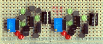
jean-paul said:I only see 4 LED's on the PCB, that's why I ask. In your schematic I see 5 LED's ( 3 green ones and 2 red ones ).
BTW since the servo is omitted maybe it is better to use an output cap + resistor to ground after it ? Could you repeat the adjustment procedure in this thread for those that don't know the Search function ? 😉
edit: I checked again and I now see that there are 2 LED's D3 in the schematic ...
Can you please answer my questions Rudolf ?
Re: Re: Why did I ask ?
Peter also has 3 green leds
It seems that the other D3 is a green led
jean-paul said:
Can you please answer my questions Rudolf ?
Peter also has 3 green leds
It seems that the other D3 is a green led
It seems like he answered the LED question here:
I didn't test my board yet.
rbroer said:
You could use a 4148 diode, but I used a green LED...think like Christmas trees
I didn't test my board yet.
Jean Paul.. Maybe it's eye exam time.. On Rudolf's pcb photo on thread #3.. I clearly see 8 LEDs.. 4 are red 4 are green.. don't know why you don't see these little things. Big mystery😀
Who needs an eye exam ?!?! In the schematic there are 2 red and 3 green LEDs per channel, OK ? Then I look at the pic of Rudolfs PCB and I see 4 red and 4 green LEDs total. Mmm that should have been 4 red and 6 green ones if the schematic is right. Scott, you say that you clearly see 8 LEDs on Rudolfs PCB. I hope you agree with me that that should have been 10 in total for both channels according to the schematic.
Check for yourself please if what I am saying is right. The confusion became bigger after me asking what diode D3 is because there are 2 pieces D3 in the schematic....
Peter has 6 green and 4 red LEDs on his Veroboard 😕
He probably followed the schematic like I did.
Confusing to me, maybe to others as well. I don't care about schematics but the picture confuses me.
I think I'll stick with opamps 😉
Rudolf is known for installing some components on the bottom side. Maybe it's the case this time?😉
Maybe one of the LEDs was hiding behind a capacitor on the picture 😀
Indeed, I suggest to stick to opamps or passive, much better and less confusion 😉
BTW, for more confusion, the current board has:
8 red LEDs
2 4148 diodes

Peter,
I'm just soldering a SE version that only needs a plus rail,
and uses cheap bjts. Cascodes on current source and common base transistor.
Will let you know how it sounds, and maybe post it as well since I'm using vero-board this time, in stead of pcb,
so it should be easy to copy.
Indeed, I suggest to stick to opamps or passive, much better and less confusion 😉
BTW, for more confusion, the current board has:
8 red LEDs
2 4148 diodes
Peter,
I'm just soldering a SE version that only needs a plus rail,
and uses cheap bjts. Cascodes on current source and common base transistor.
Will let you know how it sounds, and maybe post it as well since I'm using vero-board this time, in stead of pcb,
so it should be easy to copy.
Indeed, I suggest to stick to opamps or passive, much better and less confusion
BTW, for more confusion, the current board has:
8 red LEDs
2 4148 diodes
You are right about the confusion around your design. I take your advice on opamps or passive. No red light in my cdplayer 😉
- Status
- Not open for further replies.
- Home
- Source & Line
- Digital Source
- "Super-Pair" I/V for TDA1543