To understand the speed up cap:
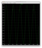
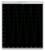
Run the sim and display the output sinewave.
Hover over the cap and click to display the current.
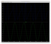
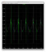
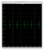
Note the smooth peaks to about 30 mA, a good amount of current.
When the driver turns on it forward biases the connected outputs and without the cap reverse biases (to turn off) the other side through the 51 ohm resistor. The cap makes a more solid connection, the duration of the effect of the speed up cap is extended with a larger value. It is clear that the cap has a powerful effect as seen by the high peak current.
Next, hover to see the current in one of the power transistor emitter resistors, top and bottom. Notice how the current is a very clean half sine as it should be.
Clip out the speed up cap, rerun the sim and look again at the somewhat distorted current due to mutual conduction.
Thanks for the useful explanations.
I looked at this and took a couple or screenshots (attached).
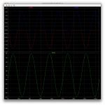
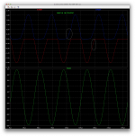
I can see how the output's currents are much better with it, but how come the current in the cap is so chaotic?
How do you choose the optimal cap value?
This would logically work more and more with rising frequency and basically do nothing near DC.
I circled those areas on the plot where the current looks odd without that cap.
That's it right?
Did you take a peek at what the signal looks like in the path along the way?
It starts looking ugly right from the start at the ltp, and I suspect this is to quickly correct for defects arising further down and coming back via the global feedback.
So it wouldn't be the ltp that's causing all that distortion and spikes, it's just preemptively acting to correct what's going on further, and the output signal looks ok. Although obviously some artifacts must be remaining and that's what the high thd reflects.
Attachments
Sim can't find 1N4004 model if you changed them all to C then it would use the Cordell.
2N3055 is still a duplicate model.
It worked on my end from that folder, but I must have that diode in my main ltspice library, so it didn't complain. It's easy to add an ako to keep it simple.
And I think there is a 3055 model that comes with ltspice, which must be the one conflicting. And that model is a simplified one from ST, with few parameters. An ako is probably also the best way to fix this.
I was curious about my devices and their breakdown voltages, so I kept on going with that tester to find out.
And wow! Most of them hold a whole lot more than I would've thought.
Except for one 3055H which doesn't even hold the 60V, it only came up for 54V, it's not good for amps, all of the other 3055s, regardless for where they came from, can hold more than 100V, and I had a few that can hold over 200V. Geez!
Same surprise with the bdx20, some come up with something like 175 for example, which for 140V devices isn't overly high, but many are well over 200V.
And even more with the 2n3442, also 140V devices, with one third of them holding over 300V, and the rest are all well over 200V and some over 250V.
A few of the 3055s didn't go over 120V, so they wouldn't qualify as mj15015, but they still were well over 100V anyway.
So no troubles going for +-35V rails on regular amps, and should be fine for much more than +-60V on the leach superamp.
The main issue is more with dissipation, not second breakdown.
And since all those devices are holding far more than their advertised 60V Vce0, they must be the newer types (epitaxial), which are at least rated for Ft at 2.5mhz.
I would not make any assumptions just because they have high breakdown voltage,
the 2n3773 was high voltage and single diffused.
Have you seen this?
RCA Transistor Oral History Meisel Page3
the 2n3773 was high voltage and single diffused.
Have you seen this?
RCA Transistor Oral History Meisel Page3
I would not make any assumptions just because they have high breakdown voltage, the 2n3773 was high voltage and single diffused.
What do you mean? Not trust those results? Or something else besides the breakdown voltage reading to think about?
Have you seen this?
RCA Transistor Oral History Meisel Page3
Interesting stuff.
I just watched a few days ago an old documentary about the period when the very first transistor was created. When the transistor didn't exist and when those guys were really toiling hard to make one work.
It wasn't quite straightforward, and they really figured out the theory behind it, knowing it should work, and yet, it wouldn't, for some time. That was quite a quest. But it was well worth the effort. And that really pushed the vacuum tubes back afterwards.
What about our superleach design? Can we make it work better?
If we can make it work right, then the protections can be tested...
I would not jump to these conclusions, you could test the Ft if you have the equipment:
And since all those devices are holding far more than their advertised 60V Vce0, they must be the newer types (epitaxial), which are at least rated for Ft at 2.5mhz.
Also, the 2n3773s with no company logo are very suspicious all reputable companies want
to advertise their brand.
I'll try to get back to the sims when I have a chance.
Thanks for the useful explanations.
I looked at this and took a couple or screenshots (attached).
I can see how the output's currents are much better with it, but how come the current in the cap is so chaotic?
How do you choose the optimal cap value?
This would logically work more and more with rising frequency and basically do nothing near DC.
I circled those areas on the plot where the current looks odd without that cap.
That's it right?
Did you take a peek at what the signal looks like in the path along the way?
It starts looking ugly right from the start at the ltp, and I suspect this is to quickly correct for defects arising further down and coming back via the global feedback.
So it wouldn't be the ltp that's causing all that distortion and spikes, it's just preemptively acting to correct what's going on further, and the output signal looks ok. Although obviously some artifacts must be remaining and that's what the high thd reflects.
There is no optimal value for the cap, large enough to avoid cross conduction.
At very low freq, the changes are slow enough so that the resistor discharges the
junction capacitances fast enough, as freq goes up so does the rate of change and
then it needs help from the cap. Yes the circled areas are correct.
Is this a sim of SIMPLE, NEW, or yours?
I would not jump to these conclusions, you could test the Ft if you have the equipment:
I don't. At least I don't think so for that type of stuff.
If I wanted to rig something basic, what would I need?
Not sure how to do this type of measurement.
And since all those devices are holding far more than their advertised 60V Vce0, they must be the newer types (epitaxial), which are at least rated for Ft at 2.5mhz.
That was my conclusion. They must all be suitable for amps.
I found 4 more of the 3055s that were desoldered from something long ago. I cleaned up left over solder on their legs so I could test them without damaging the sockets, and they're also coming up excellent and in good health.
One from SGS, obviously before the merger, measured at 126V, the others are RCA, but all above 130V, plus a BDX18 at 112V. Not too shabby.
Also, the 2n3773s with no company logo are very suspicious all reputable companies want to advertise their brand.
Yes, too suspicious and I'm not planning to make amps with those.
They seem to test fine for breakdown voltage, although I only tested very few. I have many, but I'll leave them aside for now. Perhaps in some power supply they would do fine, maybe, if they have enough of a chip inside, as the fakes usually don't stand much because of an overly small chip.
I'll try to get back to the sims when I have a chance.
Cool! It would be great if this ends up working right. Next would be pcb design time...
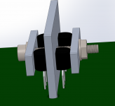
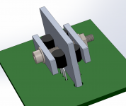
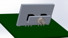
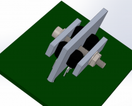
BTW: I have been giving some thought about an arrangement for DUAL LTP stages, such as what's in the leach and a lot of others, where they all could be more closely thermally coupled, by being together on a single small sink, with a little simple clamping mechanism.
There aren't any such heatsinks available out there, that I know of, allowing this, and it really needs to be simple, so it can be made by a diyer with fairly basic means and cheap.
So I did a little cad drawing and I'm posting what I came up with.
Time for positive critic and find the eventual flaws...
Attachments
-
 Screen Shot 2017-03-19 at 2.28.16 PM.png213.5 KB · Views: 59
 -
 Screen Shot 2017-03-19 at 2.27.09 PM.png206.1 KB · Views: 60
 -
 Screen Shot 2017-03-19 at 2.26.48 PM.png121.2 KB · Views: 58
 -
 Screen Shot 2017-03-19 at 2.26.20 PM.png88.6 KB · Views: 67
 -
 Screen Shot 2017-03-19 at 2.25.45 PM.png168.1 KB · Views: 55
 -
 Screen Shot 2017-03-19 at 2.25.20 PM.png120.3 KB · Views: 102
 -
 Screen Shot 2017-03-19 at 2.24.54 PM.png229.8 KB · Views: 107
That actually makes a lot of sense for any inputs biased hot, and used in lower level
stages where the heat significantly hurts noise performance. I was thinking of using
the copper shims that sell on ebay in a very similar way. I doubt it would be needed
in a power amp, yes perhaps to keep them at the same temp, in that case it could be
very small.
What is your design/engineering background? You do nice CAD work by the way.
Is this a sim of SIMPLE, NEW, or yours?
That was from the simple one.
I was wondering if the cross-conduction at high frequency, such as 20k, would be short lived and show up as spikes.
If this is more or less the way it happens, then those spikes we see all over the place inside of the loop along the signal's path would likely be just that, and being so high and numerous, the feedback isn't enough to smooth them all out, which would explain the high thd that just won't come down.
I suspect if we can tame whatever the cause is for those spikes, then thd would drop drastically, and the amp overall would be far more stable.
I think with this going on, even though from outside of the loop it looks stable and the tian probe reports excellent reserves of phase and gain, when something comes in to disturb this shaky balance, it would likely oscillate wildly.
When there is a short and the protection activates, everything goes haywire, and oscillations start all over the place. I've seen this in other sim and it's highly likely it will happen in those.
That's why whatever we can do to get rid of those oddities is bound to help with the out of the ordinary situations, like shorts or overly hard loads.
That actually makes a lot of sense for any inputs biased hot, and used in lower level stages where the heat significantly hurts noise performance. I was thinking of using the copper shims that sell on ebay in a very similar way. I doubt it would be needed in a power amp, yes perhaps to keep them at the same temp, in that case it could be very small.
It wouldn't help too much with dissipation for fairly low bias currents, but when we start having tails at some 6mA and more, some heat can build up a little in those small to92s.
But I didn't aim for a high dissipation sink. It would dissipate quite a bit more than just leaving the to92s in free air, but that wasn't the main goal.
The main idea behind this is equalizing the temperatures among all 4 devices, with a good thermal link, and keep it simple to make.
Of course using copper is definitely better than aluminum, if someone has pieces of it, why not using that instead?
But still, aluminum would work nicely as well, and even better if anodized black, for extra dissipation capabilities.
Even with low amounts of heat dissipated, the little extra sink would help keeping the parts cooler than they would be in free air, and the most important is they would be much closer in temp to each other. That is the whole point.
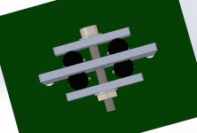
Few try to thermally link each side of a dual ltp topo. Sometimes some might at least try to couple each pair, but I would go one step further and link both pairs.
It could also be done with the current sources, but that gets more complicated and crowded.
What is your design/engineering background? You do nice CAD work by the way.
Thanks, but this is nothing extraordinary.
I'm into many things, but my main thing has always been electronics, since the age of about 13 (long ago).
I try to make use of certain tools to make things easier. So after simulating in ltspice, next step is pcb design with eagle, associated with sketchup to check things out often during the design, and then into cad mechanical for the rest.
It comes in handy. I can't get all latest software, but even a few generations behind it works fine.
The copper shims are on ebay for laptop cooling and are already cut to size.
Builders put them face to face with a zip tie, yes it is better to do all four.
Builders put them face to face with a zip tie, yes it is better to do all four.
It is possible that the spikes are a simulation issue, it seems to be mainly on one side
which led me to believe that it was an output model problem. I tried Bob C's MJs
and then it does it on both sides.
It looks more to me like crossover distortion correction however it also looks to be oscillating,
probably local? Not sure. It could be that Ic drops too much, so does Ft then the loop goes
unstable briefly. This is a guess, you'd have to verify it.
Look at the VAS current, notice how it peaks much more than normal at the peaks of the
output waveform - it is correcting for probably beta droop in the output transistors, or still
being close to clipping.
You mentioned distortion going up with more bias and lower Z, - you have a source
impedance .1 R built into your power source and so it has less headroom as you up
the bias or use lower Z loads. I would make it an ideal source which makes the resistors
then unneeded to the front end - short them.
Then open the feedback loop at HF by shorting the feedback resistor to ground, keeping a
large cap. Lower the input voltage to .018 or something that avoids clipping.
Open up the TMC feedback the VAS and output protection.
Now probe to find the source of the spikes, it cannot be feedback, power supply, protection.
If it still oscillates with the spikes then it is probably local to some transistors.
The copper shims are on ebay for laptop cooling and are already cut to size.
Builders put them face to face with a zip tie, yes it is better to do all four.
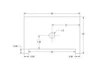
Yes, I took a look at what's available. It seems most are 15x15mm or 20x20mm, with various thickness available, but most are too think. It would have to be something like at least 1mm, or 1,5mm would be better. I drew it for 2mm, because anything thinner would make it too flexible and flimsy.
There must be sizes available in 30x20mm or something like that, in 2mm thick.
I put out a flat drawing with dimensions from that design (attached).
Quite simple to make, and with very basic tools. The hole needs to be in the right place and the notch at the bottom can be filed. If the rectangular plates have their corners overly rounded, it would make it difficult to have the little legs at each end once the notch is filed away.
I think it's good to have those notches, along with their corresponding holes in the pcb, so it can be held in place while assembling, and it's always properly positioned.
With the little legs passing through the pcb, it is held straight and prevents too much bending and stresses on the cases. Once the 2 little braces are bolted on each side, everything is well in place and there is no reason for it to move.
If the main shim is made with copper, the little legs can even be slightly longer, so a bit more sticks out from the bottom in the pcb, and with proper pcb layout with pads around the 3mm holes going to ground, the sink could be soldered and grounded.
If the shim is copper, it's probably a good idea to make everything else copper as well, including the washers, nut and screw, to avoid any eventual issues with bi-metal interactions. Plus the electrical contact is better with copper, so in the case of a soldered and grounded shim, the whole thing is then properly grounded.
It's very small, no wouldn't waste much pcb real estate.
And best of all, it's rather easy and cheap to make.
Someone with more tools would push it a tiny bit further and give a shape to the 2 little braces, so they would not bend as much when tightening the screw, and at the same time embrace the TO92s more snugly and keep them in place more precisely, preventing any chance of moving, especially during assembly.
At the time to assemble this, all is needed is a tiny bit of thermal paste, as a thin film on the TO92 flat faces.
I think for practical purposes, it's probably best to put everything in place without soldering the trannies first. And in the case of a copper shim with longer through hole legs, it could be soldered in place first, then the TO92s put in place, but not soldered, then the screw tightened and finally the trannies could be soldered last.
Attachments
It is possible that the spikes are a simulation issue, it seems to be mainly on one side which led me to believe that it was an output model problem. I tried Bob C's MJs and then it does it on both sides.
I've been seeing this on both sides, and there are many spikes, not just a couple per cycle that look like their happening at crossover. But I've seen this many times in many other sims, so it's a common occurrence.
It looks more to me like crossover distortion correction however it also looks to be oscillating, probably local? Not sure. It could be that Ic drops too much, so does Ft then the loop goes unstable briefly. This is a guess, you'd have to verify it.
The thing is, it's doing this a lot with legit signal levels, and although the feedback helps a lot in smoothing that out, what would happen in extreme conditions, such as a short on the output?
I would think those wild behaviors would go totally out of control in such situations, so we're likely to see much more oscillations when the protections activate, or when driving complex reactive loads, or very low impedance loads.
Look at the VAS current, notice how it peaks much more than normal at the peaks of the output waveform - it is correcting for probably beta droop in the output transistors, or still being close to clipping.
Yes, everything along the way looks like it's preemptively acting to correct things, starting right at the ltp, so we end up with a decent looking signal on the output, but everything looks really wild all the way through.
Obviously the result is somewhat fine, although thd does show something is wrong, and that says how much the feedback has been fighting to correct things, but not fully suppressing all defects.
You mentioned distortion going up with more bias and lower Z, - you have a source impedance .1 R built into your power source and so it has less headroom as you up the bias or use lower Z loads.
Yes, I try to make the rails less ideal, although probably nowhere near as bad as the real ones would be, with the sagging, rippling, etc...
I would make it an ideal source which makes the resistors then unneeded to the front end - short them.
What I do sometimes, is temporarily add voltage sources to the front end, so whatever the output side is doing, it's not affecting the rails for the front end.
Then open the feedback loop at HF by shorting the feedback resistor to ground, keeping a large cap.
Sorry but I'm not quite following that part. How do you short the feedback res to ground without putting the negative input to ground along with it?
Perhaps I'm not understanding which feedback res you're referring to. I assume the one coming from the output. Shorting to ground the end from the output shorts the output, and shorting the other end shorts the negative input to ground.
So that can't be it.
Lower the input voltage to .018 or something that avoids clipping.
So basically disable the feedback and make the amp work with an open loop.
I'm not sure how much open loop gain we have right now, but it's enough to really move on a tiny input signal.
Open up the TMC feedback the VAS and output protection.
So this doesn't pertain to those few latest versions posted. Since you mention TMC, this must be about that other version I recently posted with 4 output sets, where I switched the comp scheme to TMC.
I'll poke around...
"Then open the feedback loop at HF by shorting the feedback resistor to ground, keeping a large cap."
I should have been more specific, short across the feedback resistor in the path to ground.
I should have been more specific, short across the feedback resistor in the path to ground.
"Then open the feedback loop at HF by shorting the feedback resistor to ground, keeping a large cap."
I should have been more specific, short across the feedback resistor in the path to ground.
Ok, so the other feedback res then.
What I was trying was to simply disconnect the feedback altogether, and put the in- input straight to ground, leaving the feedback loop open, but then the open loop gain being sizable, the slightest signal and offset on the input sends the output to one of the rails. So since the input network also brings in its own little "disturbance", I disabled that as well and used a voltage source directly on the in+ in put.
So I had to give it a small offset, almost 1mV to bring the output's offset to a small amount, and then gave it a tiny signal to drive it to a large enough output level. It takes a good 20mV to drive it that way.
And then I saw how some spikes, far larger than the legit signal itself, are appearing right from the start at the ltp. This isn't easy.
I figured instead of adding a short on that feedback res, it was quicker to just give it a tiny value, so I gave it 0.001m. Close enough to a short.
And in that sim, with the 4 output sets, that big feedback cap is at 4700u, giving it a rather low frequency rolloff. (enough?)
I'll try that and see what I can get.
Alright, I disabled the protections, disconnected the vas limiter completely so it wouldn't bother anything.
Made the rails more ideal and instead of shorting the 2 res on the rails, I added 2 more sources for the front end, so there should be nothing going on there on those rails.
With the feedback res at .001m and leaving the big cap at 4700u, at 20khz, it takes 22mV for a significant output level, but not near clipping.
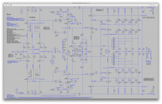
I'm posting the whole schematic, so we can be sure we're talking about the same thing. This is the 4 output sets version with the leach altered compensation, replaced by tmc, which I disconnected from the output, but left the caps in place, which leaves a low value of regular miller comp in place, and that sim also has a comp cap on the vas emitter res R23/C10 as discussed much earlier, which helps getting a decent phase/gain margin (80deg/24db).
We get a fairly clean signal on the output, despite the lack of global feedback. We do have some level of miller and other inner feedback, which is probably helping a bit. But like my other previous attempt at opening the loop, we do get spikes.
This works better than my previous attempt, as the amp's offset remains tiny.
Looking at the current coming out right from the first ltp transistor, Q1, there are already small hints of spikes, but somewhat small and few.
Then looking at the current going into the vas, all hell breaks loose, and we can't even distinguish a legit signal, because it's all such large very short spikes.
Funny thing is, this is probably reduced by the miller comp, and so the vas output current (Q22) shows at least a sizable legit signal we can recognize, mixed up in there, but full of spikes, much larger than the signal itself. And further, looking at the voltage there in that same spot (Q22's col/N018), the legit signal is there and no spikes are visible.
So current is way out of whack, while the voltage coming out looks fairly ok.
This stuff then can't be coming from the output stages. There may be more such things going on in there in the output stages, but mixed up with what comes from the previous stages, hard to tell the difference.
So is this due to the circuit or are we seeing things created by the simulation only? Are the models a cause?
The models are cordell's. For the input and vas that is. Not the outputs, and the drivers are the ones that came with the original leach amp's sim, which I slightly tweaked for VAF.
Made the rails more ideal and instead of shorting the 2 res on the rails, I added 2 more sources for the front end, so there should be nothing going on there on those rails.
With the feedback res at .001m and leaving the big cap at 4700u, at 20khz, it takes 22mV for a significant output level, but not near clipping.
I'm posting the whole schematic, so we can be sure we're talking about the same thing. This is the 4 output sets version with the leach altered compensation, replaced by tmc, which I disconnected from the output, but left the caps in place, which leaves a low value of regular miller comp in place, and that sim also has a comp cap on the vas emitter res R23/C10 as discussed much earlier, which helps getting a decent phase/gain margin (80deg/24db).
We get a fairly clean signal on the output, despite the lack of global feedback. We do have some level of miller and other inner feedback, which is probably helping a bit. But like my other previous attempt at opening the loop, we do get spikes.
This works better than my previous attempt, as the amp's offset remains tiny.
Looking at the current coming out right from the first ltp transistor, Q1, there are already small hints of spikes, but somewhat small and few.
Then looking at the current going into the vas, all hell breaks loose, and we can't even distinguish a legit signal, because it's all such large very short spikes.
Funny thing is, this is probably reduced by the miller comp, and so the vas output current (Q22) shows at least a sizable legit signal we can recognize, mixed up in there, but full of spikes, much larger than the signal itself. And further, looking at the voltage there in that same spot (Q22's col/N018), the legit signal is there and no spikes are visible.
So current is way out of whack, while the voltage coming out looks fairly ok.
This stuff then can't be coming from the output stages. There may be more such things going on in there in the output stages, but mixed up with what comes from the previous stages, hard to tell the difference.
So is this due to the circuit or are we seeing things created by the simulation only? Are the models a cause?
The models are cordell's. For the input and vas that is. Not the outputs, and the drivers are the ones that came with the original leach amp's sim, which I slightly tweaked for VAF.
Attachments
-
 Screen Shot 2017-03-20 at 2.19.49 PM.png147.8 KB · Views: 56
 -
 Screen Shot 2017-03-20 at 2.19.31 PM.png111.3 KB · Views: 98
 -
 Screen Shot 2017-03-20 at 2.19.07 PM.png176.5 KB · Views: 101
 -
 Screen Shot 2017-03-20 at 2.18.25 PM.png161.5 KB · Views: 107
 -
 Screen Shot 2017-03-20 at 2.18.14 PM.png743 KB · Views: 110
 -
 Screen Shot 2017-03-20 at 2.20.54 PM.png158.5 KB · Views: 67
Just in case, I disabled the C9 cap on the global feedback, to see if that was bringing something in from the output, but it didn't make any difference.
I thought about completely breaking the feedback loop so R18 would not bring anything from the output to the front end, but that would be like my previous attempt, and I'd have to deal with offset issues, with the in- input floating.
Those spikes must be caused by something. Is it only due to the sim? Or would a real world circuit have this too?
I'd keep the feedback in to keep the DC offset in check.
I didn't look to see if you have the double precision option set, or if the
timestep etc. is good in your sim. I'm not an expert on these settings.
Are you on the Yahoo LTSpice forum, I joined but have not been there in years.
Are all your models Cordell's except outputs, or are the input devices C grade?
You could detach the output stage and take the feedback from the VAS or predriver output.
- Home
- Amplifiers
- Solid State
- Super Leach amp simulation woes