I'm going to go on the assumption that if you build with those old parts, that you'll use at least the 2 MHz + Ft versions only. I'm fairly certain that if a part is labelled MJ2955 it is intended to meet the Motorola now Onsemi spec, can't say the same for all 2N3055s
Sure. The MJs are more likely than not to be the newer types, although at the youngest, they would be from the mid 80s.
And the 3055s from ST, perhaps even from SGS before they merged, might be from that same period. And that may apply as well to the thomson made.
(ST is SGS+Thomson, and Sescosem also a part of it)
Besides, like I said, this is more than just a personal only project, it's meant for sharing, and there are quite a few interested parties out there.
And it's also a good challenge. Making this work.
Posting my updated spreadsheet with the added comments on the parameters.
This can be useful to learn more about what each parameter does and how they relate to each other.
The sheet can also be used for more devices, so it can be a tool to tweak the models, not just for 3055s.
I marked in bold green the parameters that are in the models but with the default values. Obviously those could just be omitted, or better yet, get a real value, other than the default.
Comparing them side by side is rather educational. And some of the values start to stand out as possibly preposterous...
Attachments
The date code 8532 is 32 week of 1985.
Those are fairly new and I'm not sure if RCA ever went to a different process.
I don't think that MOT ever made slow ones.
Those 2N3773's look fake to me. I consulted for a company doing counterfeit analysis
and the first step is to see if the markings come off with acetone or alcohol. Also the
font could give a hint.
I would not doubt if all those 2n3055s would pass a 100V Vce if they are from the 1980s.
The H's should be 90 or 100V by spec.
Note also, that from the start they were rated at 60V with the base open, but with a 100 ohm
resistor to the emitter the rating was 70V.
Last edited:
Do you check distortion in the error log? There are warnings there of multiple definitions
of transistors etc., this should be cleaned up. I might have introduced them when I made
the library changes.
Considering distortion, you don't usually rate an amps power right below clipping the
performance of the parts is so bad at low Vce you just can't expect low THD.
First step was to lower vin to 2.3 for about 49 Vp out.
Next I removed the jumper across the feedback cap, DC offset increases distortion.
I think that the 220R was high because Leach did not have high current drivers, I lowered
it to 51 ohms, lowered the 330s to 150, added a Self "speed up" cap across the 51R that
gets rid of glitching in the output stage.
Lowered VAS degen from 390 to 100 R. I like to run the drivers and VAS with a decent amount
of current but try to keep the Pdiss to reasonable levels. These changes gave about 1.5W in
the drivers and about .5 in pre and VAS. I rebiased the outputs for about 50 - 70 mA, go lower
if you want to save heat/power.
The Leach amp never had low distortion at HF, I seem to remember .5% even with modern
parts. I noticed that there was attenuation in the FR at 20 KHz and narrowed this down to
the 47pF which I reduced to 10pF. It needs more feedback to clean up the output stage
so I removed the 180 pF, and added 10pF across the feedback resistor. There is still not
enough loop gain for HF distortion reduction, I added .5uF across the VAS degen, this
makes it more like a Self design at HF. All these changes led to a 20 KHz THD of about
.21%, and much less at 1KHz.
It is not finished, HF stability needs to be looked at, behavior into low Z and shorts, SOA
analysis. The PLB NEW amp should come close to this.
I seem to remember you mentioning 2 ohms, I would not attempt it with less than 16
MJ2955 type output devices and I would not go much over 70V on the rails.
Amps should be designed for 100 deg F ambient if you ask me, so keep that in mind when
sizing heat sinks unless you are planing to require a room with AC, even 110F.
Attachments
The date code 8532 is 32 week of 1985.
I knew that, but some date codes aren't as straightforward, so I have doubts.
Those are fairly new and I'm not sure if RCA ever went to a different process. I don't think that MOT ever made slow ones.
Some of those Mot are from the 70s. It all depends on when they started making the newer ones.
Even SGS and Thomson may have been making the newer ones before merging as ST.
Sescosem predates this by quite a bit, so it's not impossible that theirs were the older types.
Among the few Mot devices that I have, they have the E and B marked below, and this was done mostly in the early days, and they stopped doing it later.
Those 2N3773's look fake to me. I consulted for a company doing counterfeit analysis and the first step is to see if the markings come off with acetone or alcohol. Also the font could give a hint.
They are rather old, and I figured they could be from before the fakes were around. But it's not impossible, maybe early counterfeits.
I'll have to try some things to check them out. I have close to 60 of those.
Maybe one of them was slightly used and perhaps I could venture into cutting odd the top, to see its guts. Those don't lie, when they're fake, the guts tell all.
I would not doubt if all those 2n3055s would pass a 100V Vce if they are from the 1980s. The H's should be 90 or 100V by spec.
It's all dependent on when they started making the new ones, so who knows?
I have doubts about those H, but I hope they're legit. The specs definitely was for 100V Vce0 back then.
Note also, that from the start they were rated at 60V with the base open, but with a 100 ohm resistor to the emitter the rating was 70V.
I always wondered what they meant for VceR. It's always higher than Vce0.
Why would they stand better the voltage that way?
I want to have something reliable to test for those secondary breakdown. It's tricky to do this non-destructively, but can be done.
One other thing, I assume none of the 3055 models are of the older types.
btw: I didn't take photos of those, but I also have a few of the early possible 3055 complementaries, the BDX18 and probably some are BDX18N.
In those days I think the MJ2955s were almost impossible to find.
I'm not going to get into SPICE model work, especially on the 2N3055, I took a look at doing
other devices and it is just not worth it right now. I sense that you believe that there is a
just right or correct model.
I worked in ASIC design for a major semiconductor company, and we did all our timing
analysis over PVT. Process variation, Voltage (+/-10%) and Temperature (comm or military
range). A design was not released to fab until it passed in simulation. The process variation
is very large so what is the correct model? In fact, we did all this analysis before layout and
then again after layout with capacitance and metal delays back annotated into the model.
We should have, high, low, and typical beta, should we have more for high, low and typical Ft? How much further do you want to go?
Do you check distortion in the error log?
Of course, that's the only place to look for that info.
There are warnings there of multiple definitions of transistors etc., this should be cleaned up. I might have introduced them when I made the library changes.
I didn't pay attention to those dupes. They're pretty harmless, but it may imply the wrong one is actually being used. I will have to clean this up.
Considering distortion, you don't usually rate an amps power right below clipping the performance of the parts is so bad at low Vce you just can't expect low THD.
Perhaps not, but it is still a good indication for whatever may be going on.
Most of my sims showed pretty good thd even right before clipping starts, but not for any of the leach amp's incarnation so far.
My bryston clone with 3055s has really nice performance, all the way up.
Of couse once the first hint of clipping appears, thd goes haywire, but that's normal. I usually set the max level at the highest one before the thd starts climbing, and it's almost always very close to the clipping point.
First step was to lower vin to 2.3 for about 49 Vp out.
I had tried that, more or less, I think I tried 1.8, 1.9, 2, 2.05, 2.1, 2.2, etc... Looking for how thd evolves. And it's been much higher than pretty much any other sim I've done.
Next I removed the jumper across the feedback cap, DC offset increases distortion.
True, and at the same time, the cap introduces distortion at the low end.
But it's got to be there in the real amp anyway.
I think that the 220R was high because Leach did not have high current drivers, I lowered it to 51 ohms, lowered the 330s to 150, added a Self "speed up" cap across the 51R that gets rid of glitching in the output stage.
Those are among the things I tried on sims. I did this lately on that 4 device sets version, and it does indeed help.
The speed up cap is one thing I mentioned I'd like to learn more about, how to size it just right. It's there to help with dealing with the devices capacitance. So how do we know what the right size is?
Lowered VAS degen from 390 to 100 R. I like to run the drivers and VAS with a decent amount of current but try to keep the Pdiss to reasonable levels. These changes gave about 1.5W in the drivers and about .5 in pre and VAS. I rebiased the outputs for about 50 - 70 mA, go lower if you want to save heat/power.
I aimed for 25-30mA in the drivers in that 4 device set version, and I try not to push the bias in the outputs much beyond about 100mA usually.
We have rather low rails, especially with the device stacking, so idle dissipation isn't too much of an issue.
What's going to be important is the thermal control, and I really don't like rigging diodes through a heatsink. So an other bias spreader needs to be devised.
The Leach amp never had low distortion at HF, I seem to remember .5% even with modern parts.
That's what I've been seeing, and actually not just HF. It may get better at lower freq, but not really that much.
I noticed that there was attenuation in the FR at 20 KHz
What was that?
and narrowed this down to the 47pF which I reduced to 10pF. It needs more feedback to clean up the output stage so I removed the 180 pF, and added 10pF across the feedback resistor.
So you've tweaked those nested loops then.
The output stage indeed requires some cleanup. So the low open loop gain doesn't help that, and that's why the thd isn't stellar.
There is still not enough loop gain for HF distortion reduction, I added .5uF across the VAS degen, this makes it more like a Self design at HF.
One thing I did try and it helped quite a bit, is to do enhanced vas, as Self also suggests. And the boost in gain helps ridding some more of the distortion.
When I tried converting the stacked vas to the hawksford cascode, I gave it some more idle current and added the extra tranny for an enhanced vas. This can help to drop thd some more.
At some point, at 20khz, I managed to drop thd to just below 100ppm. (on the 4 device sets version)
All these changes led to a 20 KHz THD of about .21%, and much less at 1KHz.
Getting better, but this would be good to drop one more order of magnitude, or better if we can.
It is not finished, HF stability needs to be looked at, behavior into low Z and shorts, SOA analysis. The PLB NEW amp should come close to this.
Yes. It's getting there. We'll have to add the protections and see how that fares.
But I can say that when I enable the protections on that 4 sets sim, the thd almost doubles, even when the protections are very far from acting, and the sensing res values were chosen specifically high to have the least impact possible when present.
I tried at some point the baker clamp on the vas when sticking was happening, but it didn't do much, and when I saw the behavior was gone, I removed those. (bav21)
I seem to remember you mentioning 2 ohms, I would not attempt it with less than 16 MJ2955 type output devices and I would not go much over 70V on the rails.
I wasn't referring to a regular 2ohms speaker load, but going on the assumption that taking half a nominal load as resistive represents the worst case scenario for a reactive load, so from that, if the amp was to be bridged on a nominal 8ohms reactive load, then each amp side sees a 4ohms nominal, and taking half of that as worst case for maximum reactive load, was the reason for the 2ohms resistive value.
And that was why I have been looking at the 4 device sets version, because then the soa is just about right. (4x4 16 devices)
Plus I stayed with the 60V rails, so no deliberate plan to violate the limits set by specs, although we know the newer devices wouldn't have much trouble handling it. It's more a matter of dissipation afterwards. As long as we can make the protection act strongly enough to have sufficient fold back effect, the soa shouldn't get violated (much).
That's been the big issue with the protections. They do work, and act sort of properly but not enough, and making them start acting earlier only helps partially, all while making them even more intrusive.
I wish there was a better way to do VI protections.
Amps should be designed for 100 deg F ambient if you ask me, so keep that in mind when sizing heat sinks unless you are planing to require a room with AC, even 110F.
Oh boy! You're thinking Florida!!! 😱
Well, it depends on where and how the amp would be used. If the use is in the area where I currently am, there is no freaking way the ambient temp would get anywhere near that, unless the amp was all racked up with others in a tight space without enough ventilation.
It just doesn't get that hot over here.
But I look at soa in sim with a derating at a 50C rise on the sink as being ultimate max, and then when sizing up the sink, I just overbuild, always...
I haven't run any heatsinking calculations for this one yet, it's not even fully functional for now, but the type of sink I've been eyeing are the single flanged ones from conrad, and my little heatsink space experiment from earlier with cad drawings, showed that the 20cm long sinks can handle 6 devices easily, and so it would take 2 of those for a super amp with 3 sets, then although I haven't tried that yet, the 4 sets version likely would fit fine on the 30cm long sinks, with also 2 of them.
Those sinks have thermal res of 0.6C/W and 0.37C/W. Not too bad, and maybe could be enough. Calculations will tell.
If not enough with the 2 20cm sinks for the 3 device sets version, then it can always go on the 30cm long ones.
if that's the case, then the 4 sets version may have an issue even with the 30cm long ones, or maybe not...
If there was a real dissipation issue, then there is always the option of forced ventilation, but it gets a bit more complicated, and costly.
One thing to do is avoid all extra unwarranted thermal junctions, so those who always design their sinks with an aluminum corner that then gets bolted on the sink itself, adding a large junction in the process, should think twice and get a better heatsink choice.
No matter how much sloppy thermal paste is splattered on those corners and sinks to merge them together, it's still a sizable thermal junction, that should be avoided.
I'm not going to get into SPICE model work, especially on the 2N3055, I took a look at doing other devices and it is just not worth it right now. I sense that you believe that there is a just right or correct model.
Well, a typical average one, mostly representative of what is encountered is all we need.
We should have, high, low, and typical beta, should we have more for high, low and typical Ft? How much further do you want to go?
I wouldn't go that far. Just find a reasonable typical average.
I wouldn't have enough devices probably to make a decent matching in this case, but in other builds I would make sure to have a large enough batch to make the best sets I can get.
This is fairly unlikely to be feasible with so many needed parts from a batch that's not very much larger than the needs.
The models don't need to be representing all possibilities. we don't need to make separate ones for various possibilities, just find a rational compromise, possibly close to the datasheet speced typical values, depending on how the real parts actually are.
I may in fact not have that many 3055s with the old specs after all anyway.
There is still not enough loop gain for HF distortion reduction, I added .5uF across the VAS degen, this makes it more like a Self design at HF.
Why not encompassing both res there?
And I just realized it's 500n, which is a rather high value for compensation. I never go that high for comp caps. Why does it need it that high?
I will look at this further tomorrow, I'm about to crash. I will clean up the warnings, and I have to fix the loop probe that disappeared.
The global feedback loop has changed so it's much less a leach now.
Can make a decent 3055 based leach clone...
But the stacked devices will need to come back though.
Clean up the error log issues and set it up for distortion and I'll take a closer look at my
NEW file if you want.
I used .5uF because that's what was needed to lower the distortion at 20 KHz. Why would
you think you can do an order of magnitude better than what a Leach does with modern
parts? If you want that then you don't want a Leach.
I did not go across the sense resistor for the clamp because the clamp will not work at HF
in that case.
Dear sir
I have completed my leach amplifier but that is dead plz sugest me how can i measure voltages step by step to know fault.thanks
I have completed my leach amplifier but that is dead plz sugest me how can i measure voltages step by step to know fault.thanks
Dear sir
I have completed my leach amplifier but that is dead plz sugest me how can i measure voltages step by step to know fault.thanks
Please start a new thread and tell us more about how it failed and what it is doing now.
Clean up the error log issues and set it up for distortion and I'll take a closer look at my NEW file if you want.
Alright. A little house keeping, and it's attached. It didn't need that much though.
I used .5uF because that's what was needed to lower the distortion at 20 KHz.
Most of the time, bigger cap values equates to more distortion, but occasionally they correct something that causes more reduction than the increase they bring in, so I guess this is one of those cases.
It's just that I rarely use comp caps that big, and the larger ones are usually at the output stages. It just seemed high for the vas that's all. But if it works, of course.
Why would you think you can do an order of magnitude better than what a Leach does with modern parts? If you want that then you don't want a Leach.
Well, since there are already so many alterations to make it work better, I figured why not do a couple more to really drop thd some more. One thing I thought would help would be to enhance the vas, and one other is cascoding the vas as well. Using the hawksford cascode on the vas did help a lot in my other sim for the 4 sets version, and with those few things changed, we do get the order of magnitude thd reduction.
It doesn't fix the underlying issues, but the extra linearity and loop gain helps the feedback do more cleanup.
While you run that sim, try taking a peek at the signal at some places like on the predrivers and driver bases for example, and on the vas input. This shows how hard it is working on cleaning things up.
I did not go across the sense resistor for the clamp because the clamp will not work at HF in that case.
That's very interesting, I didn't think of that. This may be one more thing to think about when trying to get those protections to act more like they should.
Attachments
I was trying to apply a few more latest mods to my 4 sets sim to see what happens, and I found out a couple of things that I didn't realize before.
That sim has far fewer alterations to the original leach topo, at least on the output stages, where I kept his stacked topo for all 3 output stages, but with a few of the recent adjustments, like adding those BE res, getting rid of the extra emitter res, separating the device strings, and adding base stoppers.
Then the stacked vas was converted to a hawksford cascode, with an enhanced vas as in self's blameless.
This does work, with the 3055 models at hand, and I've been trying to get the protections to work on it earlier.
I had disconnected the protections because they pretty much doubled the thd when connected, even though they have no reason to be activating, on a legit signal.
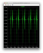
However when I was taking a closer look at how ugly the signal is in those stages, I realized that it's so full of spikes, fast transients, not from the signal but that must be generated probably somewhere in the output stages, that the protections actually are acting a little on those high spikes, and that must be why they're adding a lot of thd.
Despite that, I got that amp running on 4ohms resistive and at 20khz the thd is down well below 600ppm.
So the feedback loop is doing a great job at cleaning up all those huge spikes, so the output signal looks clean, although the thd says it's a little distorted, it's not that bad.
The better thd is earned from the extra loop gain from the vas mods obviously.
The point is, something is causing a lot of transient spikes, that are far higher in magnitude than the legit signal is.
And I noticed that when lightening up the load to 8ohms resistive, the thd drops a lot to about 66ppm, still at 20khz.
This should also say something about what's going on, by how much distortion changes from halving the load.
That sim is for 4 dev sets (16 in all), keeping leach's stacked topo, except for the conversion to cascode on the vas.
One more thing I noticed, and it's intriguing. When I lowered the bias, I saw thd dropping, and it's doing fine with some 10mA of bias per chain of outputs. Which makes for a very low overall amp bias, that is below 100mA total on each rail. Weird!
I bet if the origin of those spikes being generated could be identified and something could be done to stop them, then the feedback wouldn't have very much to fight against and thd would drop dramatically.
And by the way, with the few adjustments I just made on it, with that low bias and on 4ohms resistive load, the phase margin is at almost 81deg and the gain margin well over 24db.
I'm cleaning up that sim, so I can post it later on...
That sim has far fewer alterations to the original leach topo, at least on the output stages, where I kept his stacked topo for all 3 output stages, but with a few of the recent adjustments, like adding those BE res, getting rid of the extra emitter res, separating the device strings, and adding base stoppers.
Then the stacked vas was converted to a hawksford cascode, with an enhanced vas as in self's blameless.
This does work, with the 3055 models at hand, and I've been trying to get the protections to work on it earlier.
I had disconnected the protections because they pretty much doubled the thd when connected, even though they have no reason to be activating, on a legit signal.
However when I was taking a closer look at how ugly the signal is in those stages, I realized that it's so full of spikes, fast transients, not from the signal but that must be generated probably somewhere in the output stages, that the protections actually are acting a little on those high spikes, and that must be why they're adding a lot of thd.
Despite that, I got that amp running on 4ohms resistive and at 20khz the thd is down well below 600ppm.
So the feedback loop is doing a great job at cleaning up all those huge spikes, so the output signal looks clean, although the thd says it's a little distorted, it's not that bad.
The better thd is earned from the extra loop gain from the vas mods obviously.
The point is, something is causing a lot of transient spikes, that are far higher in magnitude than the legit signal is.
And I noticed that when lightening up the load to 8ohms resistive, the thd drops a lot to about 66ppm, still at 20khz.
This should also say something about what's going on, by how much distortion changes from halving the load.
That sim is for 4 dev sets (16 in all), keeping leach's stacked topo, except for the conversion to cascode on the vas.
One more thing I noticed, and it's intriguing. When I lowered the bias, I saw thd dropping, and it's doing fine with some 10mA of bias per chain of outputs. Which makes for a very low overall amp bias, that is below 100mA total on each rail. Weird!
I bet if the origin of those spikes being generated could be identified and something could be done to stop them, then the feedback wouldn't have very much to fight against and thd would drop dramatically.
And by the way, with the few adjustments I just made on it, with that low bias and on 4ohms resistive load, the phase margin is at almost 81deg and the gain margin well over 24db.
I'm cleaning up that sim, so I can post it later on...
Ok, for comparisons, here is that sim I mentioned for a 4 output device sets, with the protections hooked up.
As mentioned, I didn't alter leach's original topo on the output stages, I only converted the vas stack to an enhanced hawksford cascode.
I hope I gathered all the pieces right so it will run out of the box.
Using cordell's models, and the same 3055/2955 as earlier (tweaked VAF).
The output signal looks fine, and thd isn't too bad compared to our other versions, and this is on 4ohms resistive load.
When going to 8ohms, thd drops a lot.
The thd dropping so much between 4 and 8ohms should be telling something.
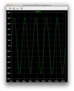
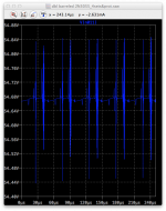
But the bulk of the thd has to be coming from those huge spikes. Take a look at those plots, from the vas output (pretty ugly), and then at vas input, from the ltp (blue trace plot).
This really shows how hard the feedback is working to clean up the signal.
It's quite stable, as the original leach, with very comfortable margins, but something is going on inside that isn't so pretty.
And by the way, the bias in the outputs is at some 10mA, and increasing this bias increases thd. Go figure!
As mentioned, I didn't alter leach's original topo on the output stages, I only converted the vas stack to an enhanced hawksford cascode.
I hope I gathered all the pieces right so it will run out of the box.
Using cordell's models, and the same 3055/2955 as earlier (tweaked VAF).
The output signal looks fine, and thd isn't too bad compared to our other versions, and this is on 4ohms resistive load.
When going to 8ohms, thd drops a lot.
The thd dropping so much between 4 and 8ohms should be telling something.
But the bulk of the thd has to be coming from those huge spikes. Take a look at those plots, from the vas output (pretty ugly), and then at vas input, from the ltp (blue trace plot).
This really shows how hard the feedback is working to clean up the signal.
It's quite stable, as the original leach, with very comfortable margins, but something is going on inside that isn't so pretty.
And by the way, the bias in the outputs is at some 10mA, and increasing this bias increases thd. Go figure!
Attachments
-
dbl barrelled 2N3055_4sets&prot.zip19.4 KB · Views: 71
-
 Screen Shot 2017-03-17 at 11.16.35 AM.png695.4 KB · Views: 158
 -
 Screen Shot 2017-03-17 at 11.16.24 AM.png106.6 KB · Views: 159
 -
 Screen Shot 2017-03-17 at 11.17.55 AM.png100.1 KB · Views: 145
 -
 Screen Shot 2017-03-17 at 11.19.21 AM.png97.1 KB · Views: 155
Last edited:
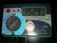
I dug out something I forgot I had, and didn't use much.
I'm not sure if it can truly be trusted, but it's giving useful info.
It's a tester called DY294, and among the tests it can perform, it does breakdown voltage, with 2 ranges, 200 and 1000V.
So I tried this out to see how this works.
I tried on a couple of my 2N3771, which are supposed to have 40V breakdown voltage, and they were well above 100V each.
Then tried a couple of those odd 3773s that are potentially fakes, just for kicks, and one gave more than 200V, the next one well over 250V.
Weird for fakes to be so far above specs.
Then the interesting part is the 3055s. I haven't tried a bunch yet, I was curious about those old Motorola marked with an "S". I wish I knew what that S means.
Anyway, I took a photo, although blurry, we can still see enough.
I pressed the hold button on the test to keep the measurement (see attached).
I wonder how trustworthy the reading is, but if it's right and they all do something like that, then I'm in pretty good shape.
More than 150V breakdown on a 3055, not bad.
Anyone knows that tester? used it?
Attachments
Those people here:
https://www.silicon-ark.co.uk/2n3055-silicon-npn-power-transistor-by-rca
Are selling the old style 3055s, at a high price, and they're targeting those who restore the old amps.
https://www.silicon-ark.co.uk/2n3055-silicon-npn-power-transistor-by-rca
Are selling the old style 3055s, at a high price, and they're targeting those who restore the old amps.
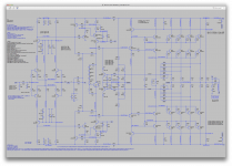
To understand the speed up cap:
Run the sim and display the output sinewave.
Hover over the cap and click to display the current.
Note the smooth peaks to about 30 mA, a good amount of current.
When the driver turns on it forward biases the connected outputs and without the cap
reverse biases (to turn off) the other side through the 51 ohm resistor. The cap makes
a more solid connection, the duration of the effect of the speed up cap is extended with
a larger value. It is clear that the cap has a powerful effect as seen by the high peak
current.
Next, hover to see the current in one of the power transistor emitter resistors, top and
bottom. Notice how the current is a very clean half sine as it should be.
Clip out the speed up cap, rerun the sim and look again at the somewhat distorted
current due to mutual conduction.
I'd probably use a film cap there.
Sim can't find 1N4004 model if you changed them all to C then it would use the Cordell.
2N3055 is still a duplicate model.
2N3055 is still a duplicate model.
- Home
- Amplifiers
- Solid State
- Super Leach amp simulation woes