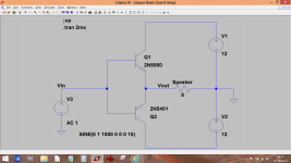
Okay, so this is a random class b amplifier....
An externally hosted image should be here but it was not working when we last tested it.
These isnt much to it. And I understand that it wouldnt sound good.
But, if I wired this up with the right transistors, would it power a speaker / head phone?
Yes it would work but there would be problems.
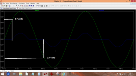
Here is your circuit together with an applied 1 volt peak to peak input voltage. Vin (the input) is the green trace and Vout (voltage across the speaker) is the blue. Do you see how the transistors do not begin to conduct until that magic 0.7 volts or so has been reached. In the case of the top NPN device the voltage has to reach +0.7 and for the lower PNP device, -0.7 volts.
So there is a dead zone around which nothing happens. In order to get music from a speaker you would have to be applying more than this -/+ 0.7 volts (so that the transistors conduct) and that is actually quite a lot. A typically music disc on a CD player would barely do that. And all you would hear would be the peaks of the signal. That in essence is crossover distortion, but in the extreme.
If you wanted to simulate this circuit all you need is LTSpice. (Click the link in my signature). If you did that we could build on it and make something workable.
Attachments
Between 0 and 0.8 volts, transistors are switches, not amplifiers. 0.6 volts off, 0.7 on, the actual switch voltage varies with temperature.
Designers "bias" transistors in the Vce zone (collector to emitter) about halfway between full on (Vcesat) and full off (collector at rail voltage), where transistors act most like a linear amplifier. To push-pull like your example, both transitors have to be "on" and passing current so some current goes between top rail and bottom rail when nothing is happening, silence. This is called the bias current. Making this bias current stable over different device temperatures is a lot of what the complications of amp circuits is all about, especially the driver and bias stages, the ones just before the output transistors.
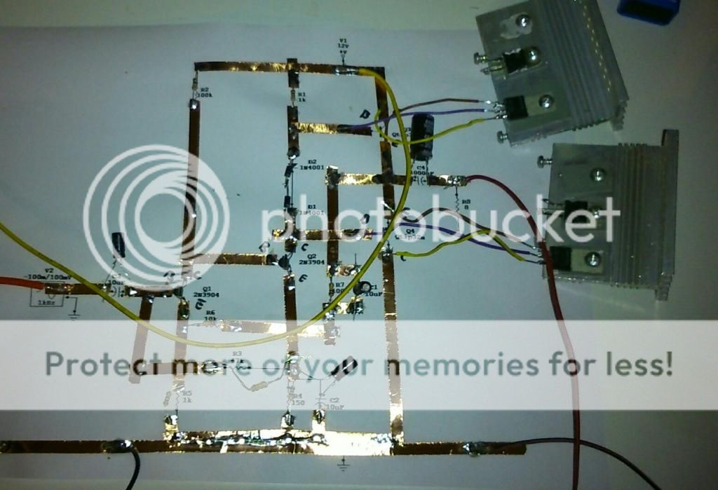
The problem with this circuit is with no emitter resistors on the outputs, things are pretty unstable. Same problem with the Red circuit in post #2. 0,3 to 0.5 ohm between the emitters and the speaker helps a lot to stabilize things. Putting the bias circuit control transistors or diodes on the same heat sink as the output transistors allows designers to use the temperature feedback to control the bias current so it doesn't run away, become infinite and toast the output transistors.
BTW the Honey Badger build document up in the sticky threads (the pdf file) has a useful explanation section that explains what all the transistors are named and what they do. Such acronyms as VAS and LTP are thrown around here all the time and before I read that I thought I was going to have to buy a hardcover book by amazon or something. I didn't build a honey badger because it is split supply and could blow up my $600 each speakers if I do something wrong and it runs away. The speaker series capacitor amps shown in many previous posts are more newby proof. My repaired amp amp with speaker capacitor produced a big ball of fire under the lectern when a solder joint let go under melting heat from the output transistors, but it didn't hurt the speakers. The junior choir was very impressed.
Designers "bias" transistors in the Vce zone (collector to emitter) about halfway between full on (Vcesat) and full off (collector at rail voltage), where transistors act most like a linear amplifier. To push-pull like your example, both transitors have to be "on" and passing current so some current goes between top rail and bottom rail when nothing is happening, silence. This is called the bias current. Making this bias current stable over different device temperatures is a lot of what the complications of amp circuits is all about, especially the driver and bias stages, the ones just before the output transistors.
The problem with this circuit is with no emitter resistors on the outputs, things are pretty unstable. Same problem with the Red circuit in post #2. 0,3 to 0.5 ohm between the emitters and the speaker helps a lot to stabilize things. Putting the bias circuit control transistors or diodes on the same heat sink as the output transistors allows designers to use the temperature feedback to control the bias current so it doesn't run away, become infinite and toast the output transistors.
BTW the Honey Badger build document up in the sticky threads (the pdf file) has a useful explanation section that explains what all the transistors are named and what they do. Such acronyms as VAS and LTP are thrown around here all the time and before I read that I thought I was going to have to buy a hardcover book by amazon or something. I didn't build a honey badger because it is split supply and could blow up my $600 each speakers if I do something wrong and it runs away. The speaker series capacitor amps shown in many previous posts are more newby proof. My repaired amp amp with speaker capacitor produced a big ball of fire under the lectern when a solder joint let go under melting heat from the output transistors, but it didn't hurt the speakers. The junior choir was very impressed.
Last edited:
Making this bias current stable over different device temperatures is a lot of what the complications of amp circuits is all about, especially the driver and bias stages, the ones just before the output transistors.
This is 100% the reason why beginners are steered toward simple low voltage class A amps and chip amp designs. In a single ended class A amp, the bias is relatively easy to stabilize (it's high all the time) and in chip amps you don't ever have to worry about it.
Using an ATX supply to "play" is just fine since they usually have short circuit protection and good regulation. There's no need to make anything more complicated than needed to do a little hands on learning.
Amazing what's in the junk bin 🙂
thank you for posting the circuit jerluwoo!
could you explain what the R7/C1 network is for, and how to design such a network?
thank you very much!
R7 is a dc feedback path to help ensure the operating point doesn't shift over time. C1 bypasses it for ac so that only R5/6 set ac gain.
Amazing what's in the junk bin 🙂
That's a cool way to prototype a circuit and easy to see whats going on. If the voltage at the output capacitor is not close to half supply (6 volts) then R4 can be increased to raise the voltage and decreased to lower it.
I started a thread over in headphone amps that uses this topology http://www.diyaudio.com/forums/headphone-systems/263801-classic-50mw.html but it seems there is little interest.
Last edited:
R7 is a dc feedback path to help ensure the operating point doesn't shift over time. C1 bypasses it for ac so that only R5/6 set ac gain.
thank you jerluwoo!
I started a thread over in headphone amps that uses this topology http://www.diyaudio.com/forums/headphone-systems/263801-classic-50mw.html but it seems there is little interest.
i've been looking at that amp for a few days now, trying to adapt it to 12v supply...
will post some questions to that thread.
Amazing what's in the junk bin 🙂
...
wow, cool!
where does one get "solderable" tapes from, and what kind?
That's a cool way to prototype a circuit and easy to see whats going on. If the voltage at the output capacitor is not close to half supply (6 volts) then R4 can be increased to raise the voltage and decreased to lower it.
I started a thread over in headphone amps that uses this topology http://www.diyaudio.com/forums/headphone-systems/263801-classic-50mw.html but it seems there is little interest.
Thanks. I'll play with that resistor.
- Status
- Not open for further replies.
- Home
- Amplifiers
- Solid State
- super basic ab amplifier?