I will put a LMK1C110x to fan the audio clock to:
This would make for a LMK1C1103 or LMK1C1104
Considering the previous discussions and work needed, I decided to extend a bit the project:
A sort of audio System On Module (SOM)...
Would you advise some important test points and solder bridges to put in that prototyping board stm32H7+USB3300?
JMF
- I2S_CKIN to drive the SAIs,
- daughter board for connected DAC,
- I propose to add to that list the TIM2 ETR, for the calculation of the USB feedback (time between SOF compared to audio MCLK ticks ; instead of SAI_MCLK). Does it makes sense?
This would make for a LMK1C1103 or LMK1C1104
Considering the previous discussions and work needed, I decided to extend a bit the project:
- switch to stm32H743VIT6 to have more audio peripherals,
- activate 3.5 SAI (in LFQP100 package, the SAI1_SD_B and SAI4_SD_B overlap without alternate options). This would give 14 channels,
- expose SPDIFRX and 2xI2S "in case it could be usefull",
- accept larger than 50x50mm PCB as not much more expensive,
- 0.1" pitch conenctors, as the more versatile for us hobbysists (discarded a digression toward high density connectors as in CM4 RPi or Portenta Arduinos)
- main connectors 8 channels usage + 2x pinheaders on the sides for the additional SAI, SPDIFRX and I2S,
- 0603 parts for manual placement and hot hair soldering, without stencil (possibly by a soldering hot plate)
A sort of audio System On Module (SOM)...
Would you advise some important test points and solder bridges to put in that prototyping board stm32H7+USB3300?
JMF
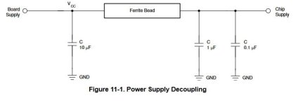
I jiust went through the LMK1C110x datasheet and it gives indications on the decoupling of the power supply (attached below). I'm not clear on how should be addressed the power supplies of the NDK oscillators and the associated buffer:
Help welcomed about good practice there.
JMF
- needs dedicated LDO for 5V to 3V3 for the 2 oscillators and the buffer?
- buffer needs decoupling from the oscillators?
- passive decoupling as per buffer datasheet OK for the 3?
- dedicated LDO + dedicated passve decoupling for the buffer?
Help welcomed about good practice there.
JMF
Attachments
Looking at the schematic in https://www.diyaudio.com/community/threads/general-purpose-dac-clock-board.413001/post-7688633, I may have some answer about my question above. Markw4 in his design has the 2 oscillators and the buffer under the same LT1763 LDO, with decoupling capacitors at oscillators. So this is one correct possibility.
I still don't grasp the key aspects of the noise propagation in the design from USB power to DAC, need for isolators and good engineering practices there. Not so good...
I still don't grasp the key aspects of the noise propagation in the design from USB power to DAC, need for isolators and good engineering practices there. Not so good...
For the oscillators decoupling caps, what would be a correct value? I see 10nF C0G 0603 proposed by bohrok here https://www.diyaudio.com/community/threads/general-purpose-dac-clock-board.413001/post-7703184. But I don't know if it is to complement a larger cap (in some design I see 10uF).
The aim is to eliminate noise from USB or MCU board to reach DAC. USB noise can be mitigated with USB isolator between host and device. MCU board noise can be mitigated by using isolators between MCU and DAC. For this to work all signals between MCU board and DAC should go through isolator (I2S, I2C, GPIO, MCK from DAC to MCU). In this case you would need several multi-channel isolators. Fast low jitter isolators are quite expensive.I still don't grasp the key aspects of the noise propagation in the design from USB power to DAC, need for isolators and good engineering practices there.
Oscillator and clock buffer decoupling is another design decision. LMK1C110X datasheet gives some advice on using ferrite beads. Their purpose is to decouple clock circuit from rest of digital circuit.
Local oscillator decoupling caps should typically have self resonance at clock frequency or at expected noise frequency. For this 10nF C0G should work well. Larger caps or caps with lower self-resonance frequency can be used in clock PSU but for local oscillator decoupling they are useless.

Thanks for the advice and the explanation on noise progagation.
About the 10nF C0G, I just found that it was indicated to use a 0.01uF cap in the NZ2520SDA datasheet, in section 8.Dimensions, in the land pattern figure. I had not seen it on first read. So fully consistent.
About noise propagation, let's start with something simple, without digital isolators, especially as I would have many signals to the DAC board. There is still the option to add such isolators on a future DAC board, possibly with dedicated power supply.
In the scenario of a USB powered DAC on the same board as the stm32 and the clocks, I imagine that the first order protections are:
Is it correct? Any other "good engeeniering" feature missing in the list?
Can the MCU control to Enable pin of the Oscillaltor be a backdoor noise entry causing issues?
If anyone is aware of article, application note, thread, web page... illustrating where the above measures get us for DAC VDD noise and DAC output noise, I would be vey interested.
JMF
About the 10nF C0G, I just found that it was indicated to use a 0.01uF cap in the NZ2520SDA datasheet, in section 8.Dimensions, in the land pattern figure. I had not seen it on first read. So fully consistent.
About noise propagation, let's start with something simple, without digital isolators, especially as I would have many signals to the DAC board. There is still the option to add such isolators on a future DAC board, possibly with dedicated power supply.
In the scenario of a USB powered DAC on the same board as the stm32 and the clocks, I imagine that the first order protections are:
- usage of LDO with High PSSR, like the TPS7A20 you suggested,
- independant LDO for the MCU, the Clocks and buffer, the DAC,
- usage of ferrite bead and 10-100nF Cap between USB connector and 5V rail (ex https://e2e.ti.com/support/processo...get-strong-noise-immunity-on-am335x-vbus-line) ?
- Cap and ferrite bead decoupling of critical loads as per LMK1C110X datasheet.
Is it correct? Any other "good engeeniering" feature missing in the list?
Can the MCU control to Enable pin of the Oscillaltor be a backdoor noise entry causing issues?
If anyone is aware of article, application note, thread, web page... illustrating where the above measures get us for DAC VDD noise and DAC output noise, I would be vey interested.
JMF
I took few days for "market" survey of the features of some recognized DACs with recommenadation on Audiosciencereview <=> good SINAD. Top performances are achieved without isolators between the USB/DAC part. Some products like the Topping D50 III or SMSL SU-1 achiece SINAD > 110 while using the USB power. So it seems that if addressed correctly, the USB noise is not so much an issue. Which reinforces bohrok addvices:
It could still be a good provision to keep the possibility to power the board from an external 5V (or above) cleaner source.
JMF
- no need to start with Isolators,
- Device can be powered from the USB.
It could still be a good provision to keep the possibility to power the board from an external 5V (or above) cleaner source.
JMF
I spent a a bit more time trying to find some application notes on USB DACs and look at some tear down on Audiosciencereview. We can see some Common Mode Line filters on data lines. Some filter between the USB connector shielding and the board ground. Even on the cheap SMSL SU-1.
I looked at the AK4493 datasheet and evaluation board, a chip that can reach very high standards. Nothing too fancy here also:
So the foreseen design does not seem should prevent achieving DAC datasheet performances 🙂
I have now to move on: finalize the schematic, complement the BOM, toute the circuit (more pitfalls there)
I looked at the AK4493 datasheet and evaluation board, a chip that can reach very high standards. Nothing too fancy here also:
- separate LDO for Digital and Analog parts,
- clock on the Analog LDO, with decoupling capacitors
- separate ground planes for the digital and analog parts, with a split in the middle of the DAC chip,
- BA033 and LT1963 LDOs, hich don't have very specific performances (Low Noise: 40μVRMS, when TPS7A20 is at 7μVRMS).
So the foreseen design does not seem should prevent achieving DAC datasheet performances 🙂
I have now to move on: finalize the schematic, complement the BOM, toute the circuit (more pitfalls there)
First of all, there is no connection between these two statements.
- no need to start with Isolators,
- Device can be powered from the USB.
(for example, all my DACs have isolators at I2S as a mandatory part, but most of them also have a USB part that is powered by USB).
Secondly, whether insulators are needed or not depends on several things. Including the use case - if you use the DAC with headphones (that is, there is no connection to other equipment), isolators can be avoided.
But when you connect different components together, especially if each one has its own main power supply, it can create a wonderful ground loop!
Small example - during the DAC debugging, I connect:
1) DAC's USB to PC.
2) DAC's output to ADC,which is connected to PC USB.
3) JTAG Debugger connected to the DAC's CPU or FPGA.
4) Oscilloscope.
Item 1 is always isolated (as I said, before).
Item 3 is not isolated.
Item 4 - the oscilloscope is very useful for debugging, but for measurements I have to turn it off (including the ground wire!)
Item 2:
When I use a non-isolated ADC, the results are catastrophic!
When I use a non-isolated ADC but with a USB isolator, everything is ok.
When I use an isolated (I2S) ADC, everything is fine.
Without a non-isolated JTAG Debugger, a non-isolated ADC can be used since there are no other non-isolated connections (one non-isolated connection does not create a ground loop, at least at low frequencies).
But sometimes you need to work with a debugger in real time in order to immediately see the results (for example, changes in register settings) in the measurements.
So once again, the need for isolators depends on many reasons and on the use cases.
Alex.
IMO the reasoning was "a USB high-speed isolator can be added externally if needed, it does not have to be a fixed internal part of the device".So once again, the need for isolators depends on many reasons and on the use cases.
No. The discussion here was about using isolator on DAC connection (I2S/I2C/GPIO). While I use such isolators on my boards I suggested that they could be left out for first revision just for simplifying the design.IMO the reasoning was "a USB high-speed isolator can be added externally if needed, it does not have to be a fixed internal part of the device".
IMO the reasoning was "a USB high-speed isolator can be added externally if needed, it does not have to be a fixed internal part of the device".
At the very least it may be more expensive compared to I2S isolation.
There can also sometimes be an issue with "totally USB powered devices", because the USB isolator itself requires a certain amount of milliamps, and the 5-5V converter used to power the external device is not 100% efficient. So there may not be enough current that can be taken from USB.
IMHO, the USB isolator is good for use with existing non-isolated devices, and when designing new ones, it is better, easier and cheaper to do it using I2S.
Alex.
I2S isolation is quite complicated for high samplerates (384+) if the controller is in I2S slave mode. The master clock should be with the codecs. If the I2S controller does not offer master clock input (so that it could work as an I2S master with external mclk signal), I2S must be in slave mode and the added isolator delay is not negligible (bclk+lrclk -> isolator delay -> I2S controller -> data out delayed by the I2S FIFO speed limits -> isolator delay).IMHO, the USB isolator is good for use with existing non-isolated devices, and when designing new ones, it is better, easier and cheaper to do it using I2S.
Of course if the I2S controller allows for external mclk, it can be run as master, and the isolator delays all outgoing signals by the same skew.
A similar problem arises for ADCs where the DATA line goes in the opposite direction, and the two-direction isolation delays will end up added instead of subtracted, if the I2S controller is in the master mode.
USB-side isolation has no issues with signals skewed by the isolator and may be more convenient in cases like this.
USB-side isolation has no issues with signals skewed by the isolator and may be more convenient in cases like this.
Sure, MCLK oscillator must be close to the DAC chip.I2S isolation is quite complicated for high samplerates (384+) if the controller is in I2S slave mode. The master clock should be with the codecs.
All other is not complicated/
Many years I use Si6261( 5+1 lines) to provide MCLK from DAC to USB-controller and WCLK, BCLK, SDATA from controller to the DAC chip if controller in master mode.
If controller in slave mode, use it opposite - MCK, WCLK, BCLK from DAC to controlled and SDATA from controller to DAC.
I've never encountered delay problems, at least on PCM384 and DSD256, in DAC and ADC.
Alex.
Both issues are solved by using I2S controller in master mode for DACs and in slave mode for ADCs. However with full-duplex mode (ADC as master and I2S controller synchronizes DAC SD to ADC) high samplerates become an issue as described in #34 (bclk+lrclk from ADC -> isolator delay -> I2S controller -> SD out -> isolator delay -> dac).
Si6261 - I am afraid I cannot find it. Did you perhaps mean the 5+1 Si8661?
Its datasheet says 10ns group delay. That's 20 ns delay for the combined direction. Period time for 384kHz 64fs data is 40ns. That means the combined delay of the isolators is half of the data period. Plus delay in the I2S controller BCLK in -> data out which for the I2S controllers I have watched on a scope (RPi4, RK3308, RK3588) is several tens of ns. IMO you are lucky that your I2S-isolated setup works OK for PCM384 and MCK, WCLK, BCLK from DAC to controller and SDATA from controller to DAC.
Its datasheet says 10ns group delay. That's 20 ns delay for the combined direction. Period time for 384kHz 64fs data is 40ns. That means the combined delay of the isolators is half of the data period. Plus delay in the I2S controller BCLK in -> data out which for the I2S controllers I have watched on a scope (RPi4, RK3308, RK3588) is several tens of ns. IMO you are lucky that your I2S-isolated setup works OK for PCM384 and MCK, WCLK, BCLK from DAC to controller and SDATA from controller to DAC.
A full duplex at 384kHz can be quite edgy even without the isolators. At 768kHz the data line gets skewed against bclk that often hacking controller vs. codec I2S format settings (clock polarity, I2S vs. left-justified) is necessary. For me if full duplex and high samplerates are required, the USB isolation is safer and easier.Yes, full duplex mode CAN be a problem, but it is solvable.
Last edited:
Si6261 - I am afraid I cannot find it. Did you perhaps mean the 5+1 Si8661?
Sorry, typo. Of course 6661 (also 6660 and 6062, if need).
Most of my DACs works with WCLK, BCLK, SDATA from controller to DAC, just MCKL from DAC to controller.IMO you are lucky that your I2S-isolated setup works OK for PCM384 and MCK, WCLK, BCLK from DAC to controller and SDATA from controller to DAC.
- Home
- Source & Line
- Digital Line Level
- STM32 USB to I2S multi channel - Hardware part