RF workers of the world unite, you have nothing to lose but your loops...
Perhaps the only one with a 200W soldering iron? 😀
At low frequencies a bus is fine. But its resistance isn't zero, so you do get voltage drops along it. The art is to get them in the right places (keep ripple current off busses). A star ground avoids this problem because none of the loops are common. At RF, the inductance of the (inevitable) long wires in a star becomes significant, so a flattened-out buss is in order. It's called a ground plane.
rdf said:Am I the only ground plane fan in the house? 🙂
Perhaps the only one with a 200W soldering iron? 😀
At low frequencies a bus is fine. But its resistance isn't zero, so you do get voltage drops along it. The art is to get them in the right places (keep ripple current off busses). A star ground avoids this problem because none of the loops are common. At RF, the inductance of the (inevitable) long wires in a star becomes significant, so a flattened-out buss is in order. It's called a ground plane.
Re: RF workers of the world unite, you have nothing to lose but your loops...
What's not to love? 🙂
I've usually only been able to effectively use a ground plane with a pcb with four or more layers (except maybe for relatively sparse layouts, like a two-sided SMPS board I make). And if the power and ground planes are close-enough together, the capacitance between them can also do wonders for decoupling the power planes, at high frequencies.
But with my practical maximum of two pcb layers for quickie homemade double-sided pcbs, I can usually only get partial ground planes, at best, with basically none of the ground plane or capacitance benefits of a "real" pcb. :-(
But, for audio-frequency stuff, I've been thinking about at least trying some sort of "pcb sandwich" or some multi-pcb/layers method, or maybe even just a closely-spaced parallel pcb, for a "sort-of" ground plane. Even if it were just to make the main pcb's layout easier to get much better, it might be well worth it. I have also been meaning to try just using an unetched board as the ground for a point-to-point build (similar to how they're often used for "dead bug"-style protos), and maybe also try using a separate pcb but with a star topology etched, which should be much easier to do well, with a whole board only for that. I guess I'll have to think about the possibilities, some more, with home construction in mind.
Actually, it seems like maybe a three-layer "pcb sandwich" for power and ground planes, with pins that mate with sockets on the "main" parallel board, could be a good approach, if using homemade pcbs. Mill-Max makes lots of neat individual pcb pins and sockets that should be very helpful. And I already have some very large carbide bits, to drill large holes where pass-throughs are needed for the lower layers. If I use thin-enough pcbs, and can find the right combination of pin and socket lengths/depths, I should be able to glue together one 2-sided board and one single-sided board, to make a nice three-layer setup for dual power rails and a ground plane, to plug into the main board.
That seems like a good, practical point of view. Maybe a star ground could also be thought of as a zero-length buss. And I sometimes like to think of a ground plane as a star ground that automagically configures itself, since, for HF at least, the return currents tend to try to flow directly under and along the paths they came by on another layer. Placement can still be important, though, to try to avoid having the wrong currents share the same return paths/areas on the ground plane.
Soldering should not be a problem, since most pcb layout software will automatically insert "thermal relief" features around solder pads on ground planes, i.e. a gap around the pad, with thin "spokes" connecting it to the plane.
rdf said:Am I the only ground plane fan in the house? 🙂
What's not to love? 🙂
I've usually only been able to effectively use a ground plane with a pcb with four or more layers (except maybe for relatively sparse layouts, like a two-sided SMPS board I make). And if the power and ground planes are close-enough together, the capacitance between them can also do wonders for decoupling the power planes, at high frequencies.
But with my practical maximum of two pcb layers for quickie homemade double-sided pcbs, I can usually only get partial ground planes, at best, with basically none of the ground plane or capacitance benefits of a "real" pcb. :-(
But, for audio-frequency stuff, I've been thinking about at least trying some sort of "pcb sandwich" or some multi-pcb/layers method, or maybe even just a closely-spaced parallel pcb, for a "sort-of" ground plane. Even if it were just to make the main pcb's layout easier to get much better, it might be well worth it. I have also been meaning to try just using an unetched board as the ground for a point-to-point build (similar to how they're often used for "dead bug"-style protos), and maybe also try using a separate pcb but with a star topology etched, which should be much easier to do well, with a whole board only for that. I guess I'll have to think about the possibilities, some more, with home construction in mind.
Actually, it seems like maybe a three-layer "pcb sandwich" for power and ground planes, with pins that mate with sockets on the "main" parallel board, could be a good approach, if using homemade pcbs. Mill-Max makes lots of neat individual pcb pins and sockets that should be very helpful. And I already have some very large carbide bits, to drill large holes where pass-throughs are needed for the lower layers. If I use thin-enough pcbs, and can find the right combination of pin and socket lengths/depths, I should be able to glue together one 2-sided board and one single-sided board, to make a nice three-layer setup for dual power rails and a ground plane, to plug into the main board.
EC8010 said:
Perhaps the only one with a 200W soldering iron? 😀
At low frequencies a bus is fine. But its resistance isn't zero, so you do get voltage drops along it. The art is to get them in the right places (keep ripple current off busses). A star ground avoids this problem because none of the loops are common. At RF, the inductance of the (inevitable) long wires in a star becomes significant, so a flattened-out buss is in order. It's called a ground plane.
That seems like a good, practical point of view. Maybe a star ground could also be thought of as a zero-length buss. And I sometimes like to think of a ground plane as a star ground that automagically configures itself, since, for HF at least, the return currents tend to try to flow directly under and along the paths they came by on another layer. Placement can still be important, though, to try to avoid having the wrong currents share the same return paths/areas on the ground plane.
Soldering should not be a problem, since most pcb layout software will automatically insert "thermal relief" features around solder pads on ground planes, i.e. a gap around the pad, with thin "spokes" connecting it to the plane.
salas said:Don't forget the matrix buss bar solution.
Is that where you wear a long leather coat and indulge in a lot of violence?
EC8010 said:
Is that where you wear a long leather coat and indulge in a lot of violence?
That's it:
"We need valves - lots of valves!"
7N7
EC8010 said:
Is that where you wear a long leather coat and indulge in a lot of violence?
Wish it was so sci fi! Its actually what richwalters always does:
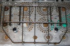
''For over 40 years in amp designs I have always used a closed earth loop concept and it works. Pic of 3.5mm bus interconneced in grid form shown for 2x150W stereo using parallel o/p pairs. With this closed bus one can be rest assured that both sides will perform symmetrically with excellent 15Khz separation performance at full power and hum isn't an issue.
Using a chassis with tags, they nearly always work loose.
richj''
Merry Christmas for everybody!
Attachments
- Status
- Not open for further replies.
- Home
- Amplifiers
- Tubes / Valves
- Star ground help