That looks nice ! Not a big problem , C13/14 might creep a little beyond the pad for a standard 33pF silver mica.
I could not find any SM packages (2mm X 3.2 mm) most are 2.5 X 3.2mm.
A better ceramic can be used here , https://www.vishay.com/docs/45258/vjhifreqseries.pdf
Many package sizes , use any 200V and up.
Here is one that will fit perfect - "exceptional HF + stability under harsh conditions" - https://www.mouser.com/ProductDetail/KEMET/C0805C330JCGACAUTO?qs=xZ/P%2Ba9zWqa07XbrwyUyaw==
2mm X1.5mm ....
Most of these IPS pads will accept multiple packages,
I have fined tuned the compensation cap pads on all the artwork to now accept that 3,2mm SM cap.
But , they are pretty expensive ( 4+$ apiece !! )
PS - here are those fancy silver mica caps ... https://www.mouser.com/c/passive-co...ance=33 pF&length=3.2 mm&voltage rating=500 V
OS
Last edited:
I was working on the BOM anyways , those components are the final candidates.
NASA has good paper on what and why modern MLCC capacitors fail -
https://nepp.nasa.gov/files/29931/N...y-Paper-NEPPWeb-BOK-Cracking-MLCC-TN65668.pdf
perhaps if we could avoid the design and sourcing issues of modern SMD parts failing , I can make better choices.
Perhaps avoid the ones that commonly fail. There is a lot of substandard junk out there !
OS
- MLCC's are by far the greatest (global) cause of circuit failure.
- Manual soldering is by far the greatest cause of MLCC failure.
Only some of the better MIL spec MLCC's can withstand touchup (a soldering iron). These have
flexible polymer termination and other special features to mitigate failure if cracks do develop.
SMD semi's (the diodes and trannies) obey the same rules as through-hole parts. But , they might be
more susceptible to board flexing /thermal shock ( no leads ).
SMD LED's and diodes also use a ceramic substrate but with that flexible conductive polymer to termination (tough).
So , since I'm new to this SMD thing .... these factors are good to consider when I choose my sources.
OS

JLCPCB have assembly options for SMT devices, it is done using BOM tools and LCSC numbers, saves a lot of time, shipping costs and eye sight for me, and prices are fairly low....Just in case, it might be one option that worth a look for you.
That's no fun ? This is DIYA , not have china do it. Who knows what parts they would (really) use ?
That heat gun looks fun , even for doing through-hole - I watched the video. I want one.
OS
That heat gun looks fun , even for doing through-hole - I watched the video. I want one.
OS
Hot plate and pan, hot air station, good tweezers and eye magnification = 🥳

Sadly ,i think that i will put my boards in the bin when they arrived.😟
Too many fine tuning after my order.
Too many fine tuning after my order.
I see it as an opportunity to gain some more experience working with modern parts. Eyesight is the most challenging for me, my 70 year old eyes cant see the difference between a SMT resistor and a grain of rice. So I will trow away all rice, and tbh I also do need a magnifying glass for TH components, so whats the difference. At some point this little board will make music for me.
I think you have the cart in front of the horse. Imo the designer should be the person verifying their design before it’s released to the public for use. I know it’s diy but you can still follow an orderly design process.
I use two irons to remove passive smt. You can use some bare copper wire formed to lay on the pads of active devices to remove them. I have a hot air machine, used it a couple of times to remove a Dfn packaged device.
Do not place a hot iron tip on the smt device terminations, put it on the pcb pads instead.
What do you mean , spooky also was built in 2015. design was verified. Clip tested and pretty square waves at 100k.I think you have the cart in front of the horse. Imo the designer should be the person verifying their design before it’s released to the public for use. I know it’s diy but you can still follow an orderly design process.
I use two irons to remove passive smt. You can use some bare copper wire formed to lay on the pads of active devices to remove them. I have a hot air machine, used it a couple of times to remove a Dfn packaged device.
Do not place a hot iron tip on the smt device terminations, put it on the pcb pads instead.
Kypton+ greenamp is the 2023 "hellraiser".
Spook and hellraiser use my present spooks(real amp) VCCS servo setup - perfect.
All the EF3's are 1980's Japan (HK) designs.
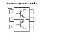
What errors ? (below) I know the fmbm5551(5401) pinout is strange ....Hi OS, I think there are two small errors on Spooky silkscreen.
pin1 = B1 , pins 1-6 = B1-E2-B2-C2-E1-C1 .... weird ? Fairchild even makes it harder
with it's BS representation.
I chose these as they are common and among the only low Cob/high Vce dual.
They spec better than the old 2N5551/5401.
The most common SOT6 pinout is like the BC817/807 with E1-B1-C2-E2-B2-C1.
One might ask why no CAD/AI assist ?
-1. Can't afford it.
-2. I've tried it on Eagle. Short of an AI trained for creep , grounding , and general style ... output
would be (Much) less than desired.
PS - I've gone over the cascode/ltp "chain" a dozen times because of those weird pinouts. Even searched
for a better device that fit spec and was common - nope.
OS
Attachments
I've never used it but I hear good things about Kicad and it's free (I think). It's supposed to compare board to schematic and do 3D rendering.
I have free access to full blown eagle with my Fusion license but I won't use that miserable piece of software! They're integrating it right into Fusion now but Diptrace still does a much better job for me.
Valery and I did a bunch of designs with mmbt series of dual packages. They had a much nicer pinout. You could rotate them 180 degrees and still have the same connections. The big downside was they were all the top heavy SC-70 package that wouldn't stay upright.
I use Kicad 7 for my vintage units replacements boards and easyeda for small boards and SMT assembly, they are nice zero cost tools, but I'm more a fixer and not a designer, and my work is nothing critical, just personal audio stuff and open source experiments.
I understand however is hard for some people to transition to other tools, particularly when they are proficient in what they use.
For SMT soldering I feel better with a soldering pencil and entry level microscope than heatgun/magnifier glass, I use it for heat shrink tho.
Anyway this are just my experiences that may or may not be useful for other's workflow and/or habits.
I switched to stencils and an oven a few years ago. Hot air works nice with a stencil too. Anything else makes for globby soldering or a lot of work with solder wick.
Which dual mmbt's ?Valery and I did a bunch of designs with mmbt series of dual packages. They had a much nicer pinout. You could rotate them 180 degrees and still have the same connections. The big downside was they were all the top heavy SC-70 package that wouldn't stay upright.
Show that. A general Stencil , or one generated from the specific Gerber ?I switched to stencils and an oven a few years ago.
I was mistaken on the dual packages. They were BC846/856. Worked great but the damn things kept flipping over. I never tried them in the oven.
They burn the stencil from the paste layer of the Gerbers. I'll upload a picture tomorrow when I'm back at the office. PCBWay burns the stencils out of stainless but Mylar works well too. There's a bit of an art to aligning the stencil but it measures the paste perfectly every time. An added bonus is the parts self align themselves in the oven due to the surface tension of the solder. Very neat finished product.
They burn the stencil from the paste layer of the Gerbers. I'll upload a picture tomorrow when I'm back at the office. PCBWay burns the stencils out of stainless but Mylar works well too. There's a bit of an art to aligning the stencil but it measures the paste perfectly every time. An added bonus is the parts self align themselves in the oven due to the surface tension of the solder. Very neat finished product.
Isn't amazing the amount of options available for create stuff on these days? It always makes giggle like a nervous teenager 😛Very neat finished product.
- Home
- Amplifiers
- Solid State
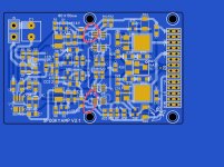
- Spooky and Hellraiser SMD 60W amps (Wolverine compatible IPS)