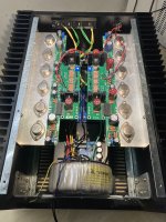
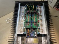
Thanks. Anyone can tell me what are C3 and C4 for? They're slowing down raising VFET Vgs at start, what is the reason for that? And they are not present in simplified DIY schematic. Can I use smaller value, say 22uf or just 10uf?
There's very useful information about this in the build guide by 6L6: Sony Vfet Illustrated build guide
" Power-up and power-down sequencing.
Back to depletion mode devices - The Vfets are normally on, right? We need to apply a bias voltage to control them. If the bias voltage isn’t there controlling current flow when the rail regulators power up, the Vfets will conduct an excessive amount of current and the 40-year old, completely irreplaceable smoke made from vintage Japanese un-obtainium, ground unicorn horn and pixie dust will escape. A sad result which will also smell bad.
So we must have the bias regulator working before the rail voltage is turned on. How did Nelson do it? A simple application of the time constant to charge 2 differently sized capacitors in the regulator circuits. The regulator with the smaller capacitor will turn on before the one with the larger cap. These caps in the race are C3 (47uF) on the bias reg and C1 (220uF) on the output regulator. It’s a 4.7-to-1 ratio and C3 will be charged about 4.7 times sooner.
The TL431 are shunt regulators, so they do not conduct current until the voltage rises to the regulation value, and then they conduct so as to hold that value.
So what about power down? The rail voltage needs to be turned off before the bias voltage. (the opposite of power-up) BUT, the big cap/small cap ratio will NOT work in our favor when shutting down. It would work exactly how you’d expect, where the small cap will discharge before the big one.
So what? The VFETs will drain the supply quickly enough, but when the supply voltage drops down quickly we may find the Gate to Source voltage (Vgs) of the Mosfet at a high enough voltage to stress the transistor into failure. It's not that likely, but everyone knows that Pass wears both a belt and suspenders to hold up his pants, and this is reflected in his design.
The fix is a simple 2-cent diode. On power down, D1 will be a very attractive and very low-resistance discharge path for C1, discharging it rapidly and turning Q7 (and Q13) off, and therefore the rail voltage to the Vfets. Because there is no special path for C3 in the bias regulator to discharge, it will operate for a longer time, which is perfectly ok."
Papa commented on decreasing C3/C4 in post #433 here:
https://www.diyaudio.com/forums/pass-labs/276711-sony-vfet-amplifier-2-a-44.html#post4412024
https://www.diyaudio.com/forums/pass-labs/276711-sony-vfet-amplifier-2-a-44.html#post4412024
It was found to be better to change the resistance rather than increase the capacitance for stability issues. For what it’s worth.
Sorry need forum help again. The amp is up and running, bias is good, test voltages are all good. BUT having 100 Hz hum pretty loud. Checking with scope gives 150mv pk-pk pure 100hz sine ripple at the amp output. Investigated further and got clear picture that hum initiated at the gates of Q15/Q16 mosfets. They are slightly overbiased, having VD across R25 of about 2.5V - shouldn't be an issue. That gives same 150mV ripple at the FE output. That's a question since DIY version have the same approach with mosfets, I built several units and have no issues whatsoever. Maybe Q11 and Q12 jfets are underbiased somehow allowing ripple to get through the pots to the mosfet gates?
OK, all done. Figured that ripple on FE out is relevant to the supply voltage. With variiac, I checked - the ripple disappears in narrow voltages window, i.e inbetween +/-29V to +/-30,5V. And its bad since we have mains voltage in +/-10% fluctuations. So, R39-R40 changed 10->33, C11 and C12 220 -> 1500uf. Got 20mv hiss, which is normal. Nevertheless, I am still believe that front end shall be powered from regulated supply...
Because of the front end(s) is it just to slap a potentiometer on the V-fet amp and be done with all my buffering needs? Or would I benefit from using a buffer preamp like the B1?
Last edited:
Hmmmm, no that would not be recommended. Because the VFET amp Output Stage has no gain (actually <1), it needs a front end with both gain and sufficient voltage swing. The kit front end has a gain of 5 by virtue of the Edcor signal transformer, which has a simple JFet buffer in front. Some of the other front ends by Mark J. have a gain of 6.1, and I have boosted a couple of mine to a gain of 7.Does that mean I can just use a pot?
Even if you have a strong preamp, it is most likely unable to deliver enough voltage to let the VFET amp deliver its rated power output.
Pass DIY Addict
Joined 2000
Paid Member
I'm thinking that amplifier models are being confused here ^^^^
Rewind's question is about the 2016 vFet-2 which uses a push-pull output topology.
Tungsten's reply seems relevant to the single ended lottery amp.
Rewind's question is about the 2016 vFet-2 which uses a push-pull output topology.
Tungsten's reply seems relevant to the single ended lottery amp.
No, I am in the wrong section. Tungsten knew intuitivelly what I meant.
Papa needs to become more inventive with the names of his V-Fet amplifiers. 😛
I have used the VFET V2 Lottery amp with a B1 Triode and never run out of steam. In fact I use it with 10% volume usually.
I ask because with the SissySiT the front end apparently is like a buffer preamp and all you need is a passive attuenutor.
But which prramp is actually recommended for VFET lottery amp V2?
Last edited:
The SissySIT front ends consist of JFet buffers driving autoformers in a 1:4 configuration. The output stages are followers.
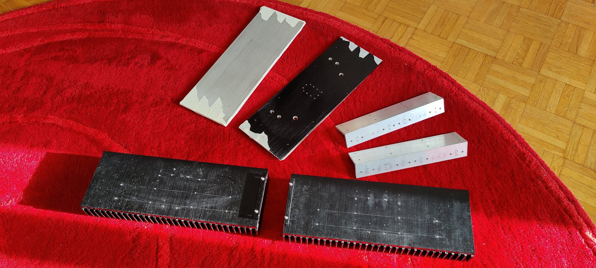
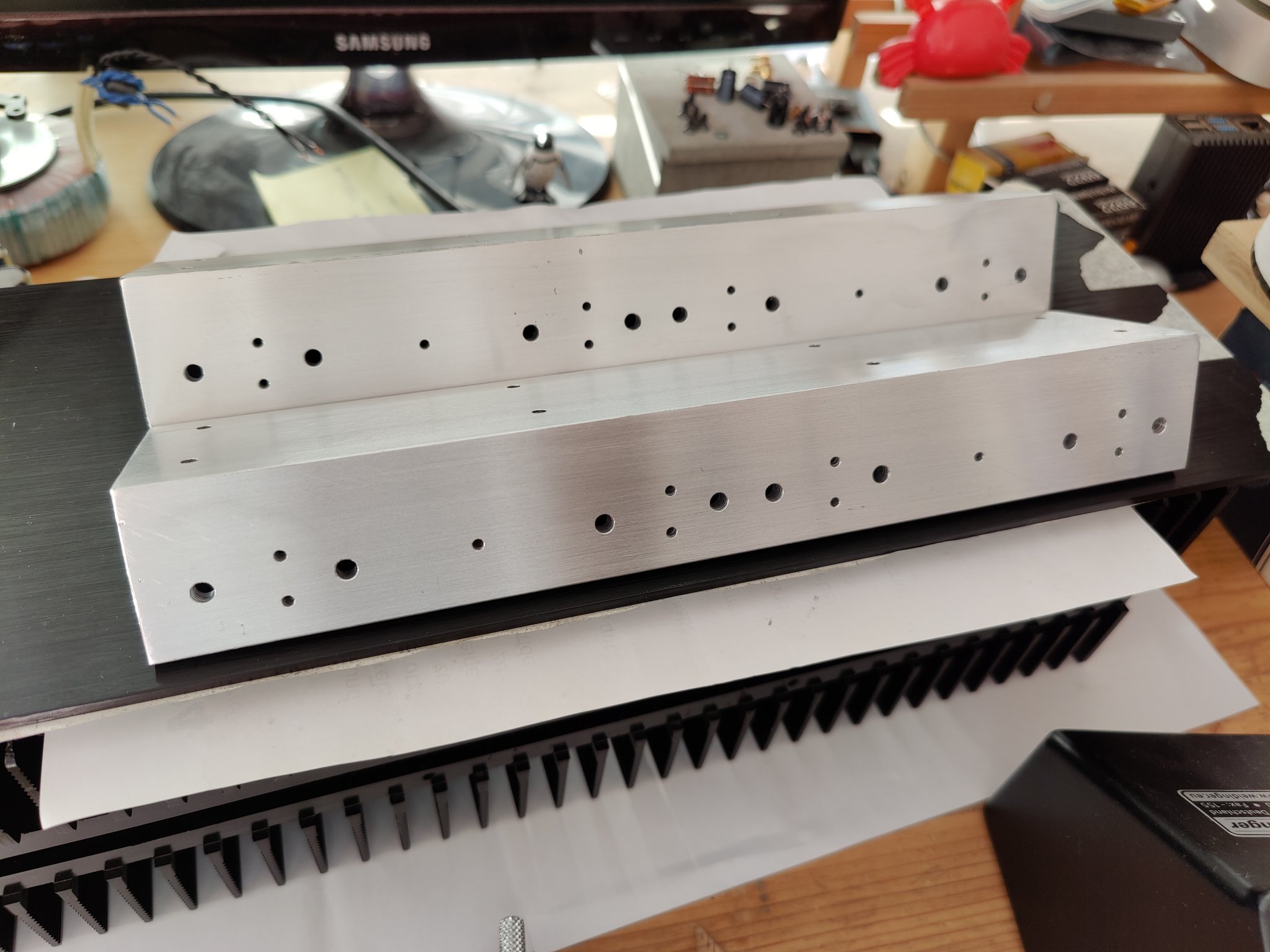
Another Sony VFET Amplifier Part 2 build with "AL" PCBs slowly coming to life. Took me ages to get moving, mostly because drilling and finishing the brackets takes a special kind of motivation that's not always easy to come by.
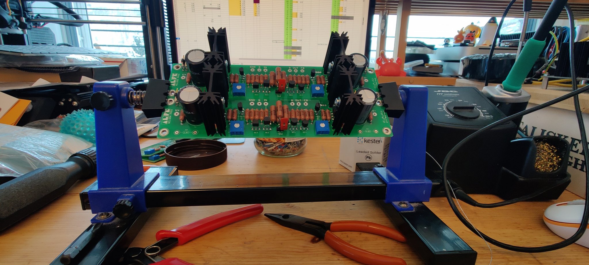
Putting together the frontend was more familiar terrain. RN60D resistors mostly, with some RN65E in the feedback network. I'm using a 5R degeneration resistor for the p-channel Jfet (and slightly higher Idss, so that it matches the N-channel with degeneration) in the frontend to make them more complementary.
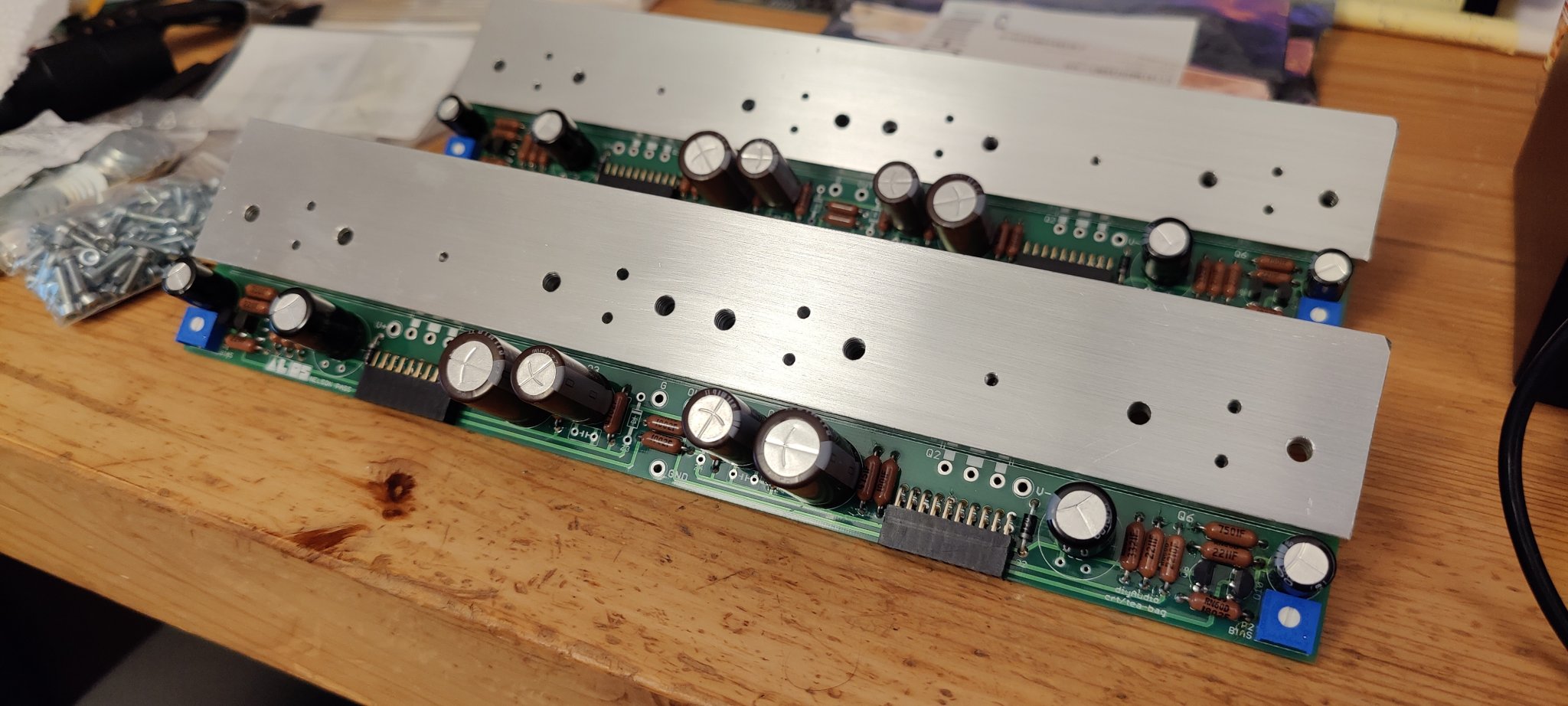
Output stages mounted to the brackets with two short screws from the back.
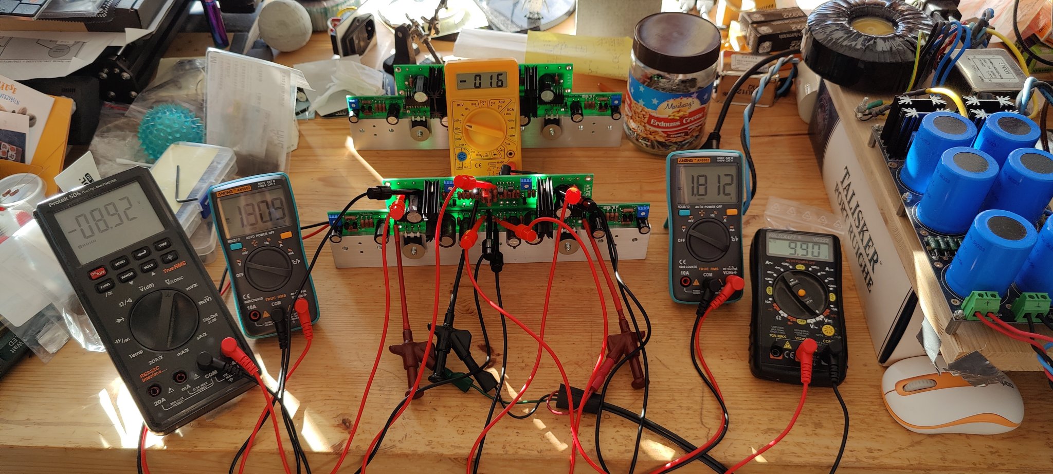
Now mated with the output stage, and powered up from a bench top PSU providing +/-28V. No smoke, and reaching all the bias points with ease (and the help of a fleet of DMMs). Final bias setup involved adding a Volt in the respective direction to the output stage bias.
No words necessary.
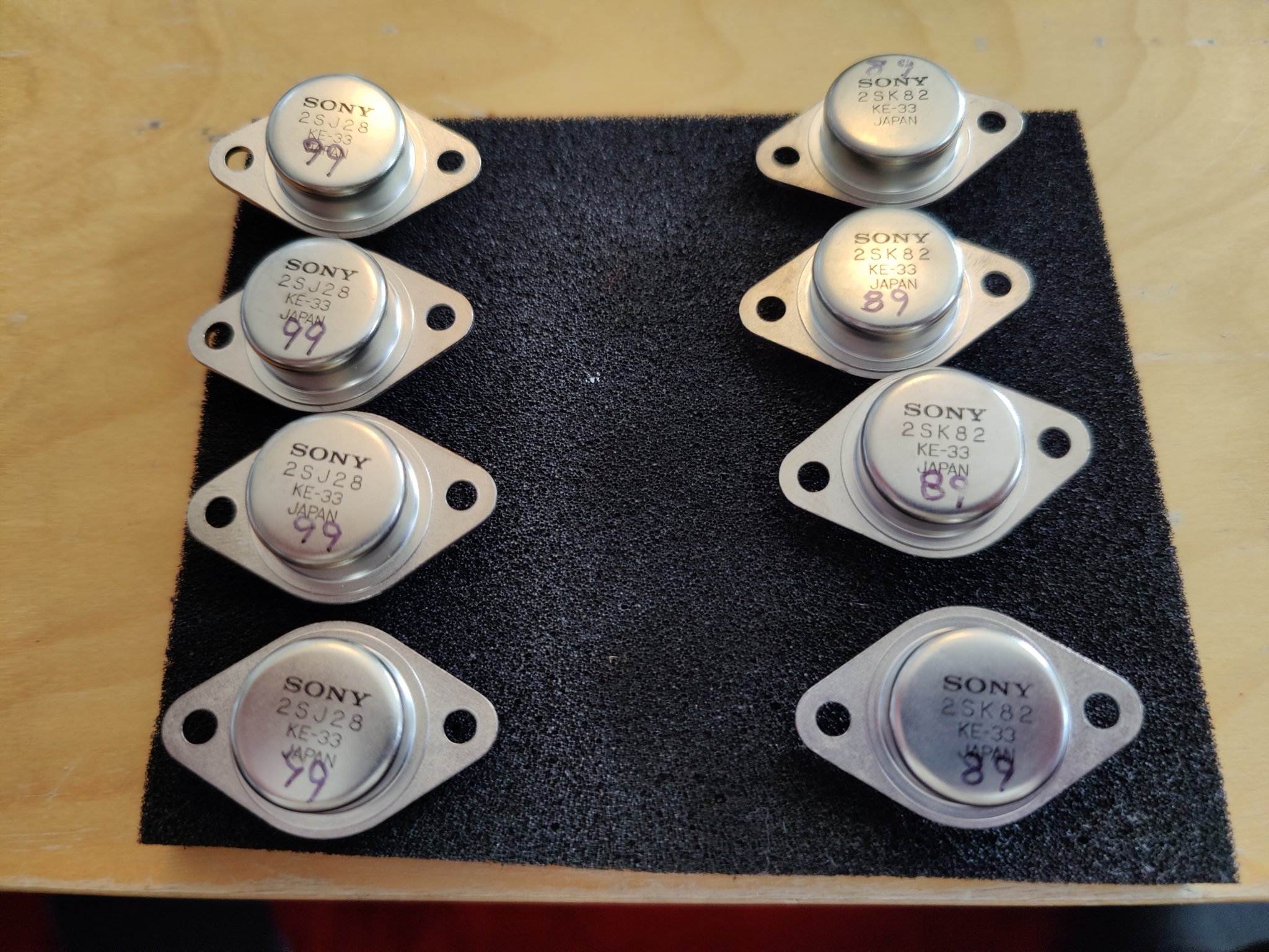
Beauty cream. (Kerafol Keratherm KP 97)
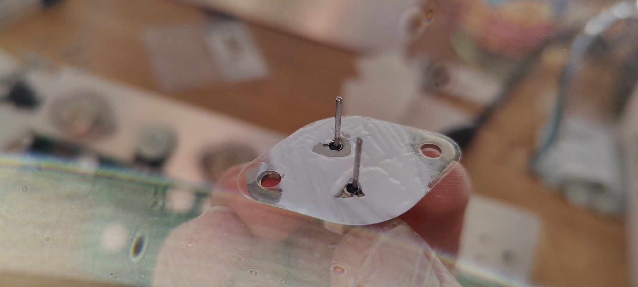
Shrunken heatshrink tubing to insulate the pins and bolts from the brackets.
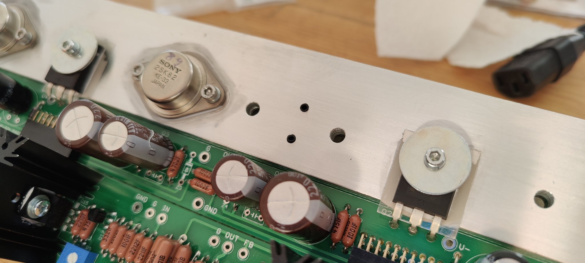
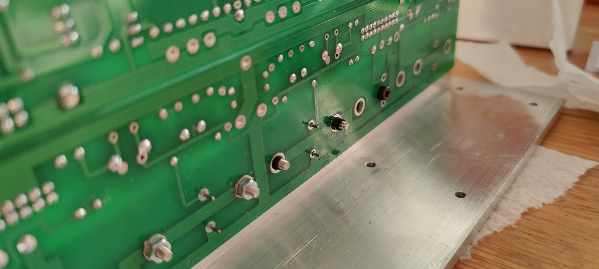
I added a tiny dash of solder to the eyelets so that the washer would make good contact with the somewhat soft solder deposit.
Done for the day 🙂
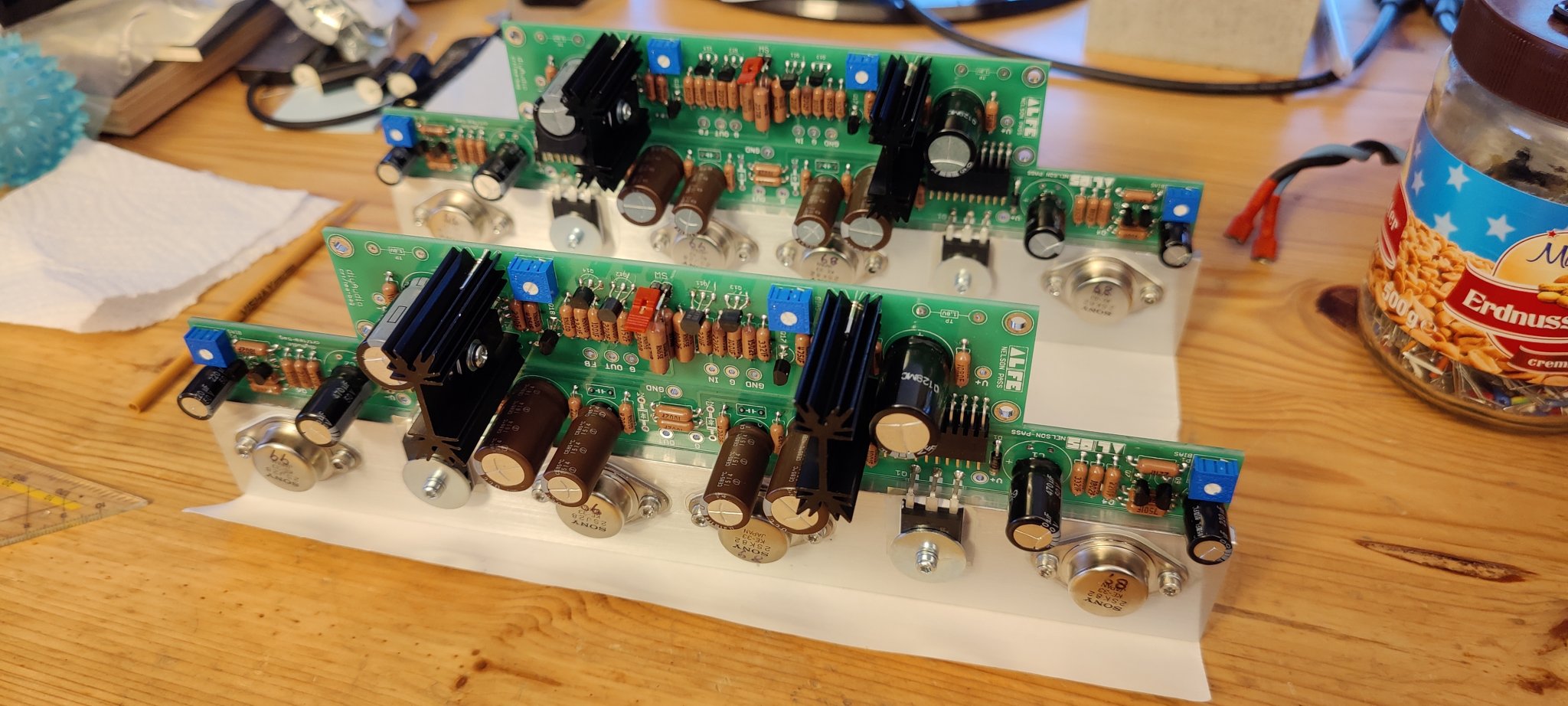
Next up is mounting the output stages to the heatsinks and biasing them up with the V-Fets in circuit.
And then on to finishing the PSU and case. Here's what the PSU will look like, CCRCC:
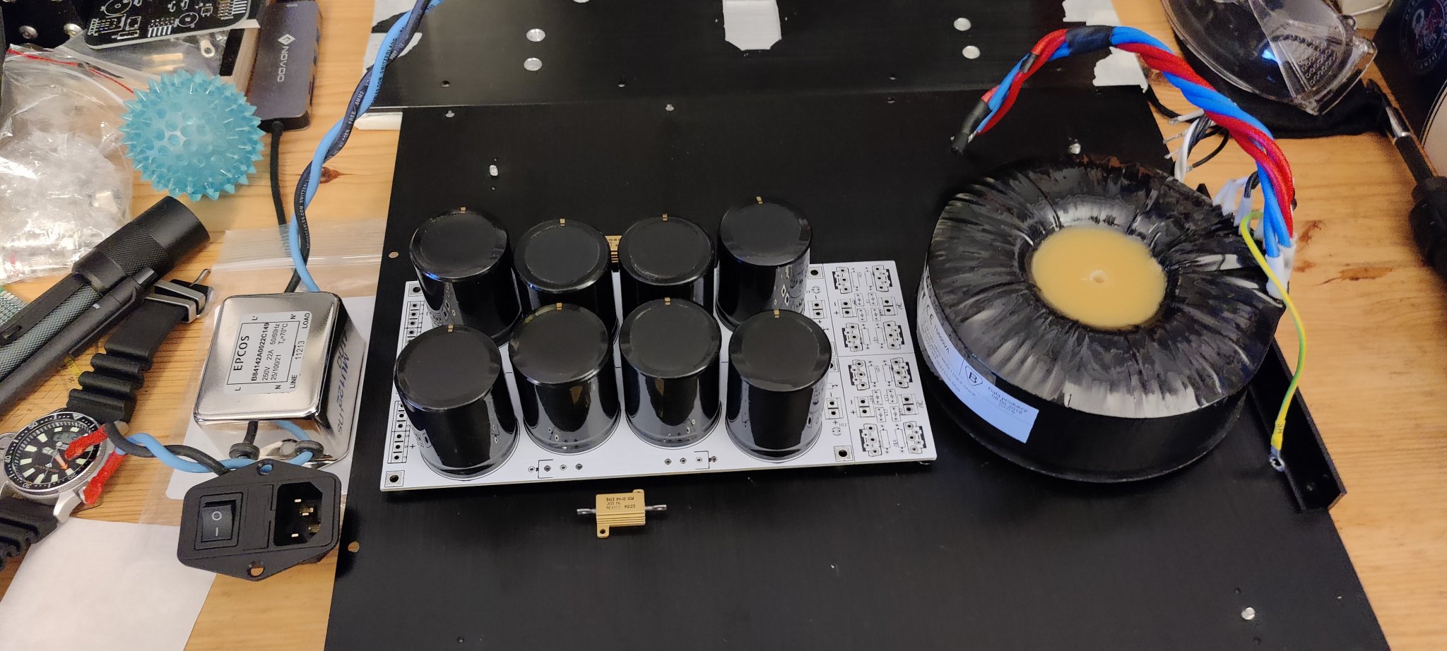
Toroidy 2x22V 600VA, 8x33000uF 35V BHC caps, 10 0R15 wirewound.
Stay tuned!
Putting together the frontend was more familiar terrain. RN60D resistors mostly, with some RN65E in the feedback network. I'm using a 5R degeneration resistor for the p-channel Jfet (and slightly higher Idss, so that it matches the N-channel with degeneration) in the frontend to make them more complementary.
Output stages mounted to the brackets with two short screws from the back.
Now mated with the output stage, and powered up from a bench top PSU providing +/-28V. No smoke, and reaching all the bias points with ease (and the help of a fleet of DMMs). Final bias setup involved adding a Volt in the respective direction to the output stage bias.
No words necessary.
Beauty cream. (Kerafol Keratherm KP 97)
Shrunken heatshrink tubing to insulate the pins and bolts from the brackets.
I added a tiny dash of solder to the eyelets so that the washer would make good contact with the somewhat soft solder deposit.
Done for the day 🙂
Next up is mounting the output stages to the heatsinks and biasing them up with the V-Fets in circuit.
And then on to finishing the PSU and case. Here's what the PSU will look like, CCRCC:
Toroidy 2x22V 600VA, 8x33000uF 35V BHC caps, 10 0R15 wirewound.
Stay tuned!
Pass DIY Addict
Joined 2000
Paid Member
Oooo-la-la! Nice looking build! I’d be curious to hear your impressions of the amp with and without feedback engaged.
I’m still sitting on parts for a CSX1 build and am curious to compare to my single pair vFet version and the single ended lottery amp.
I’m still sitting on parts for a CSX1 build and am curious to compare to my single pair vFet version and the single ended lottery amp.
- Home
- Amplifiers
- Pass Labs
- Sony vFET Amplifier Part 2

