Ahh, thanks Dennis.
I think I'm going to reorder some TL431As for my BA-2 aggrandisement. I looked in my stash and of course I have 'B' parts....
I think I'm going to reorder some TL431As for my BA-2 aggrandisement. I looked in my stash and of course I have 'B' parts....
re-adjusting bias
hi everybody!
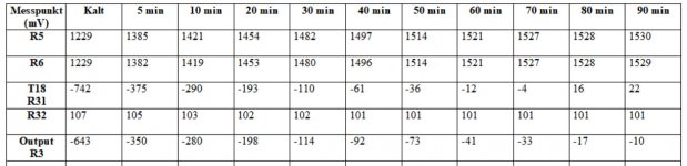
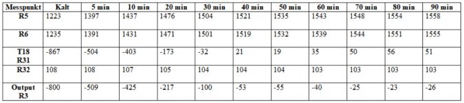
today i was wondering if there is any drift in the bias setting with the time , so i measured the amp after almost 18 months. the result : yes there is some 🙂
at the left channel T18 was drifted from initially 7mv away up to 270mv but the rest of measurements were within the range.
at the right channel T18 was around 190mv (initially 6mv) , but the output DC offset was 350mv!(initially 19mv).
so to stay on the bright side of life, it is probably good to check the bias at least once per year and re-adjust. ;-)
any similar expediences with your vfet amp?
best wishes
hi everybody!
so to stay on the bright side of life, it is probably good to check the bias at least once per year and re-adjust. ;-)
any similar expediences with your vfet amp?
best wishes
Do you use spring washers on the vfets to mount them?
It might also be worthwhile retightenting them to the heatsink.
I generally let the amp go through 3 thermal cycles of use, then once the amp has cooled down check every bolt and retighten mosfets down on heatsinks and every other bolted electrical connection.
Then recheck operating conditions, bias snd dc offset.
Kind of like what I do after a new engine rebuild on my motorbike. Hahahaha
Was there an audible cue that made you think to remeasure?
yes, indeed 🙂 ... i was facing the case that the sound stage drifts a bit to the left after 30-45 minutes of warm-up. i am keen to see if the output dc offset on the right channel caused this issue .
i have not had a new sound check yet, because i would like to re-check the bias again and maybe put another psu transformer in parallel to the existing one 🙂 ... but i will report if the issue got hopefully fixed 😉
Do you use spring washers on the vfets to mount them?
It might also be worthwhile retightenting them to the heatsink.
I generally let the amp go through 3 thermal cycles of use, then once the amp has cooled down check every bolt and retighten mosfets down on heatsinks and every other bolted electrical connection.
Then recheck operating conditions, bias snd dc offset.
Kind of like what I do after a new engine rebuild on my motorbike. Hahahaha
thanks for the hint. the housing is still open for further tunings and i will check and retighten the screws !
Pass DIY Addict
Joined 2000
Paid Member
Thanks for the report on voltage drift. I suspect it has more to do with ambient temperature than anything else. Constructing in summer and re-measuring in winter will probably be the biggest difference. Lid on vs lid off is also likely to show some difference.
Thanks for the report on voltage drift. I suspect it has more to do with ambient temperature than anything else. Constructing in summer and re-measuring in winter will probably be the biggest difference. Lid on vs lid off is also likely to show some difference.
yes, you are right; this is why the settings have to be done always with the lid on and i have been doing that as well. for that reason i use 5 DMMs for the ease of work 🙂
usually i measure the the bias every 10 minutes to get an idea how the changes are for about 90 minutes and fine adjust. the values over R32 , R5 an R6 do not change that much, but the rest (output DC, T18) continue to change and there no "saturation" even until 90 minutes. However, the most of the changes (highest slope) happen within the first 30 minutes, so i am good if i set up the amp after 60min and fine tune after 90 min. 😉
That's excellent news. Please post some pics when you have time.
(Or as the Mighty Zen Mod would say: "No porn, no glory." 😀😀😀)
(Or as the Mighty Zen Mod would say: "No porn, no glory." 😀😀😀)
Thank you Dennis,
I’m giving it a little tidy. Pics will follow.
I bought the pcbs over two years ago, as soon as I bought them I read the page again and realised you couldn’t buy the VFETs. Very glad I persevered.
I’m giving it a little tidy. Pics will follow.
I bought the pcbs over two years ago, as soon as I bought them I read the page again and realised you couldn’t buy the VFETs. Very glad I persevered.
Hi all, after a smooth build of one side of the Pass Sony Vfet I built the second side and ran into a problem. I'm at the stage of biasing the front mosfets and after doing the initial voltage checks which were all OK, R5 and R6 are totally unresponsive to P4,P3 as I try to bring them up to 1.5v. Can anyone give me an idea where to start to trouble shoot, any help would be greatly appreciated... Just to elaborate my read back from the test points are 000 on both sides
Last edited:
Hi Bugeyes,
I'm no expert, and others can certainly help you a lot more than me, but to start:
Q5 and Q6: Toshiba or Fairchilds?
P3 and P4: 500R or 1K?
Also make sure it's actually P3 and P4 you are turning and not P1 and P2. On my first module I was too focused on the DMM readings and unwittingly turned P1 and P2 instead of P3 and P4.
Paul
Thanks for the reply. Q5 and Q6 are fairchild's and per the supplemental BOM correct and the opposite functioning board correct. P3 and P4 have the correct code 501 for 500. Made sure to adjust the outside (relative to the board) pots. The inside pots, P1 and P2, worked perfectly to adjust the Vgs for the Vfets to be installed later. Made sure Q7 and Q8 were correct per the BOM...
Assuming there are no damaged parts, I guess it's possible you have a
combination of low Idss jfets and high Vgs mosfets.
Can you test/verify a few things:
1) What voltages do you measure across R35 and R34, and what value resistors do you have there?
2) Can you measure the voltage between T7 and T10 test points (ie, one probe at T7
and the other at T10) as your adjust P3 through its range? What voltage range do
you see?
3) Can you repeat 2) for T9-T12 and with P4?
Thanks,
Dennis
Dennis, in response
1.voltage drop on R35 -1.28v, R34 +1.24v both dale resistors have 221 printed on the body.
2.T7-T10 voltage swings cw -1.28 to -4.0v, T9-T12 voltage swings cw 1.27v to 4.0v
thanks for the response..
1.voltage drop on R35 -1.28v, R34 +1.24v both dale resistors have 221 printed on the body.
2.T7-T10 voltage swings cw -1.28 to -4.0v, T9-T12 voltage swings cw 1.27v to 4.0v
thanks for the response..
That range looks rather low for proper biasing of the mosfets.
I suspect you need to increase the R35/P3 and R34/P4 resistance.
Using 1K trimmers for P3/P4 will probably do it.
I suspect you need to increase the R35/P3 and R34/P4 resistance.
Using 1K trimmers for P3/P4 will probably do it.
- Home
- Amplifiers
- Pass Labs
- Sony vFET Amplifier Part 2