Maybe the next step is to work on your amplifier. You may have to do some research to get an idea of how you want to do that. 
so my smps is finnally ok! 🙂
Nice!
I'll make a search. Thanx for the help.. I've u've some idea for Amplifier... 😉
😉
Nice!
I'll make a search. Thanx for the help.. I've u've some idea for Amplifier...
😉Yes, so far it is doing well. Later you may have to rewind your transformer again. But I think you can hook up your amp to it and see what results you get first.
Later you may have to rewind your transformer again
 😱 NOOOOOOOOOOOOOOOO!
  🙂
🙂 Do u've any schematic of a poweramp?
And if i connect 2amp of 60W each for example that require +/-35V should the SMPS give +/-70V or what?
Thanx!!
 Sorry about the rewinding of the transformer, but that is how DIY is. Besides, you may want to experiment later anyway. 😉
 For two amps, you want the voltage to be the same for each of them. The positive power input of each amp goes to +30 volts, and the negative power input goes to -30 volts. Those voltages should not change much. Then you connect the speakers between the output of the amps and the common point between the power supplies, which is usually ground.
I would give you a schematic of a class D amp, but I am still designing various circuits and am unable to work at my bench and try any out for real. My next suggestion for you is to use something called a gainclone. It can use one IC chip for each channel.
ABSOLUTELY THANX FOR ALL THE HELP GAVE! WITHOUT U AND THE OTHER PPL I WILL NEVER GET THAT RESULTS!
THANX FOR ALL!
EXPECT SOME MAIL IF I'LL HAVE SOME PROBLEMS!
 KIDDING!
5 pages... WOW! 🙂
THANX FOR ALL!
EXPECT SOME MAIL IF I'LL HAVE SOME PROBLEMS!
KIDDING!5 pages... WOW! 🙂
made it myself a few weeks ago
I've made such a smps just a few weeks ago, the schematics came from rod elliot's page. Never had a problem, also used irf540. I know - and you also apparently - why rod elliot says: "You will need an oscilloscope (or at least access to one) or the project will be very much harder to build and test. A design such as this relies on careful measurements and great care to make certain that it will perform as expected. Attempting this without an oscilloscope is not recommended".
I threw out the snubber (just dissapated heat, i had no overshoot) but i altered the Pulse Width, for the safety of the expencive mosfets.
I've wound my transformer from an old pc smps to get +/-20VDC at about 150W.
My amp are 2 LM4731, one in bridge for my sub and one for 2 mids and 2 highs, whith active filtering.
I've just began with my thesis and internship at BarcoView - Avionics (www.barco.com) on the design of a 'high power buck converter with planar inductor', and now much things I didn't understand when building a car inverter and the above smps are becomming clear to me. I guess a little knowledge about these things is not a luxe for such projects (and a scope).
Sander
Your power supply and amp project seems to have turned out very well. An oscilloscope makes all the difference. Best wishes for you in the beginning of your career at BarcoView.
@fundum
while it looks nice on the bench, you should use a transformer to inject a small signal into the loop so that any disturbances will be sensed by the error amplifier, i.e. can inject noise or pulses -- emulate the real world --
while it looks nice on the bench, you should use a transformer to inject a small signal into the loop so that any disturbances will be sensed by the error amplifier, i.e. can inject noise or pulses -- emulate the real world --
subwo1
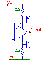
Is correct how symbol is represented?
Is correct how symbol is represented?
An externally hosted image should be here but it was not working when we last tested it.
An audio amplifier is a device which can amplify an input signal for producing audible output from a speaker. An audio driver IC reminds me of the old way medium power amplifiers were made in which the IC drove output transistors which then operated the speaker. Now-a-days one IC chip can be the entire amplifier and the output transistors are not used.
However, I have seen a nifty way that pass transistors can augment the current output capibility of the chip amp. The power transistors are operated in common emitter mode where power going into the chip amp is first passed through the base emitter junctions of the transistors whose emitters are tied to the power supply rails (common emitter configuration). The collectors of the pass transistors are connected to the output of the chip amp.
However, I have seen a nifty way that pass transistors can augment the current output capibility of the chip amp. The power transistors are operated in common emitter mode where power going into the chip amp is first passed through the base emitter junctions of the transistors whose emitters are tied to the power supply rails (common emitter configuration). The collectors of the pass transistors are connected to the output of the chip amp.
Attachments
something like this?
I've asked u this becouse i've searched on the net for IC Power amp but they're complicated to solder and i can't build a pcb...
IC like
are impossible to solder without a pcb...
So a Audio driver maybe considered a Power amp right?
An externally hosted image should be here but it was not working when we last tested it.
I've asked u this becouse i've searched on the net for IC Power amp but they're complicated to solder and i can't build a pcb...
IC like
An externally hosted image should be here but it was not working when we last tested it.
An externally hosted image should be here but it was not working when we last tested it.
are impossible to solder without a pcb...
So a Audio driver maybe considered a Power amp right?
Ahh, yes, that is the way it was popular to do it way back when. But you might be surprised that chip amps can be quite simple now-a-days. They can be done without printed circuit boards using p2p (point to point) wiring. Actually, I only build p2p circuits, and if a circuit is more complicated, I plan to build p2p modules and attach them to whatever is big and solid in the circuit that can be fastened securely. Those things include circuit breakers, transformers, filter capacitors, potentiometers, heatsinks, etc.
See, I consider circuit boards too time consuming and I don't want to sacrifice design and testing time for it. It goes without saying that I do not have any money to spare either. Besides, I prefer troubleshooting p2p because I can follow it much easier since it tends to follow the natural circuit path much more than PBC's. Also. there is no need to follow traces around like a maze puzzle or go through the layout process in the first place. One last thing to mention is that p2p circuits can be more compact than PCB's even though they use standard leaded (through-hole) components. A couple of disadvantages is that they lack the professional appearance and solidness of PCB's.
Some useful tips are to use 1/8w full leaded resistors which you can trim to the length needed for your p2p connections, Bend up every other lead on the 8 pin LM3875, for example, higher than it comes originally to give more space between pins for fitting the resistors and to provide more room for the solder. if you mess up a solder connection, heat the bad joints up and slam the assembly down to knock off the solder so that you can redo the connection(s).
Check out National Semiconductor's popular chip amp
LM1875.pdf. There can be very few components if desired. You can also bridge it AN-1192 without adding much more to the circuit. I recommend the chip in the isolated package, LM3875F, because it is easier to mount to a heatsink.
Next year I may throw together a quick circuit to see if it really is possible to boost the output current capacity by using pass devices turned on as power is drawn by the chip. The resistors bypassing the gates of the mosfets I plan to try, eg IRF510 and IRF9510, would need to be judiciously chosen. What might happen is that the distortion may be very high or the chip may go into shutdown. Resistors most certainly will be needed at the connection between the drains of the mosfets and the output pin of the LM3875F.
If anyone has experimental or simulated results on this bypass idea, it would be nice to hear what happened. I noticed that there were no SPICE models on the chip at National's Web-site.
could u explain me this? Why if i use a different transistor i've different output? And how can i determinate how much power i'll have from them from their own datasheet?
An externally hosted image should be here but it was not working when we last tested it.
- Status
- Not open for further replies.
- Home
- Amplifiers
- Class D
- SMPS problem