Yes possible😉
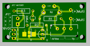
Hopefully this is all the configurations out there as Gate on side with drain and source interchangeable I think it will cover all possible 3 pin jfets out there .
Hopefully this is all the configurations out there as Gate on side with drain and source interchangeable I think it will cover all possible 3 pin jfets out there .
Attachments
Last edited:
Nice and thank you, it beats my all purpose jig that always requires 10 minutes to remind myself how it worksYes possible😉
Hopefully this is all the configurations out there as Gate on side with drain and source interchangeable I think it will cover all possible 3 pin jfets out there .

Attachments
and sure you possibly spend more money on making it. Sign up before the board finishes ,limited by 20 unless someone volunteer for a group buy.
Using this jig can probably be made faster and easier with the addition of an SMD positioning tool. For instance, a piece of card stock with an internal cutout corresponding to the general shape and size of a SOT-23 (or whatever semiconductor package needs to be tested), and attached to the SMD pad area with double-sided tape.
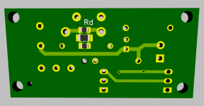
Jcarr, there is no need for any tape. The area on PCB has copper pours that will reliably do the same job. If you look carefully they are not just SOT 23 pads , but copper pours about 6 times wider than standard SOT23 pin width. Hopes that is what you are looking for with tapes.
- Status
- Not open for further replies.