Hi Jens,
what are the phase angles for the four different plots?
Are you only plotting for Tc=25degC?
I am surprised at the extent that the 4ohm exceeds the cold SOAR.
What power/current/voltage are you simulating?
what are the phase angles for the four different plots?
Are you only plotting for Tc=25degC?
I am surprised at the extent that the 4ohm exceeds the cold SOAR.
What power/current/voltage are you simulating?
Re: Daughter of Leach, Lite
slowhands:
very nice! if a group buy that meets requirements evolves, i'm interested, also.
mlloyd1
slowhands:
very nice! if a group buy that meets requirements evolves, i'm interested, also.
mlloyd1
slowhands said:See attached layout of Leach Amp, with plastic packs for a lite version. PC board is 80x100mm, or about 3.2x4 inches (half the size of the original, with no wires to the output transistors).
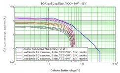
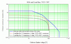
JensRasmussen said:Here are my SOA calculations
Worst case as per Self + Slone
\Jens
Jens, I had seen your graphs for the 3 and 5 pair cases, this one for 2 pair is excellent, very nice work. It does seem that using the MJL4381 and MJL4302 at 55 volts, 4 ohm reactive load the load line just touches the SOA curve. Are there other devices in the same package that would have more margin (such as the MJL21193/4)? I know you looked at many.
I suspect that a wide range of parts would serve. You are encouraged to use the ones you prefer; the design is tolerant of a wide variation. All of the parts you mention above have less beta droop and higher Ft than the MJ15003/4 in the original design, which is nice but not absolutely necessary. I suggest these for good safe operating area, because Rod Elliot recommends them highly, and because I have bought counterfeits of the 1302 and 3281, so I have a bad taste in my mouth about those particular parts. I suppose buying from a reputable distributor would allay that concern.AndrewT said:Hi Slowhands,
I agree with everything you said except one:
MJL4281/4302 is not seen as good as MJL3281/1302.
Look at the 20V & 5V vce vs DC current gain. With both the NPN and PNP the lower voltage 1302 & 3281 has about twice the current, or better, before the graph falls significantly. However the absolute gain is better with the newer pair, but they can't maintain even the same gain to those high currents.
In just about every other parameter the newer higher voltage BJTs do better.
AndrewT said:A group buy or private Emails to DIYaudio members will not exclude lurkers out to steal your layout. They will get it and reproduce it at will, if they can see a profit for themselves.
The power predictions in my later post fully confirm the obvious ability of 2pair that you had foreseen. [/B]
Yes, right. I just don't want to make it easy to steal. The layout is a lot of work, and proving the prototype is a lot of work. It would seriously annoy me if someone stole it, but I can't prevent a determined thief from doing so. It's a tradeoff between sharing enough information to illustrate the conceptual design with honest folks and keeping it locked up. For me the exchange of ideas is paramount, so I am willing to risk it.
I think we all benefit from open discussion of this. For instance, Jens contributed his SOA curves to the discussion, and they apply to any amp design you might care to do. Privately, Jens also suggested that I widen the footprint of certain capacitors for better availability, which I did. Andrew, you have provided good analysis of the SOA and of the current limiting on the VAS, as other recent examples. I am always eager to learn more, so being open about my design ideas (and being receptive to criticism) is very beneficial to me, despite the risk of copycats ripping off the design. It's not a perfect world, so I must accept the good with the bad.
Here's a link to a Motorola application note AN1308 that discusses output protection in a 100 watt amplifier using 3 pairs of 1302/3281 output pairs. I discovered this on another thread last week. Hopefully, the discussion could help someone determine the proper component values for Jens' 6 output board, which I'm still obtaining parts for. If anyone has the time and skills to translate this info into parts values for the protection circuit of Jens' boards using the above listed outputs, feel free to post the results for us, especially for 56V supply.
http://home.eunet.cz/rysanek/pdf/mot-amp2.pdf
http://home.eunet.cz/rysanek/pdf/mot-amp2.pdf
Hello,
I'm interested in PCB files too (gerber, protel, etc.) - making PCB is cheaper here - in Poland. One pair PCB (stereo) for 3 pairs Leach/Jen's amplifier cost about 50 euro (27,5 for PCBs, for prepare production docs 22,5). That 2 pairs PCB is smaller so will be more cheap...
I'm interested in PCB files too (gerber, protel, etc.) - making PCB is cheaper here - in Poland. One pair PCB (stereo) for 3 pairs Leach/Jen's amplifier cost about 50 euro (27,5 for PCBs, for prepare production docs 22,5). That 2 pairs PCB is smaller so will be more cheap...
acenovelty said:[B
You could try to get samples thru:
http://www.onsemi.com/PowerSolutions/home.do
If you sign up, they will sample you 25 each for the cost of shipping.
[/B]
They will also phone you and ask how the design's coming on, and when would be convenient for their rep to visit. They did me, anyway.
MiniLeach
The attachment here offers a minimalist pcb layout of my own that I posted some time ago in another Leach thread. It may be of some interest to those who missed it. Anybody who wants to use it is welcome. Be warned; it is a “tight” layout; not one that I would recommend for automatic insertion! I should add that the Leach protection arrangement can be implemented on this, should one wish to do so. From a professional and reliability point of view, I dislike vertically mounted power resistors, so didn’t, even though there is some “real estate” advantage to be gained. The active devices are generally as Jens’s schematic, apart from my use of 2N5551/5401 instead of MPSA42/92. I used axial polystyrene in place of mica.
In another vein, I hope it won’t be considered too audacious of me to offer some of my (possibly erroneous) observations on a tiny corner of this renowned and respected design.
Firstly, I wonder about the standard (non-Leach) Vbe multiplier bias arrangement, as is implicit in this thread, when applied to the Leach. There are six junctions +Vq (V across 2xRe’s) that the bias must overcome, but only two are exposed to the high heatsink temp. Thus a temp. coefficient of around 11.5mV/degC, instead of the required 5.6mV/degC* or so (with bias transistor attached to the power device), results in massive overbiasing after cessation of high power levels, possibly resulting in high crossover distortion until thermal equilibrium is restored. Doug Self went into this exhaustively* (and he was only referring to four junctions), and concluded with a simple idea for a variable temperature coefficient multiplier, which could reduce this effect. Strangely, though, hardly anyone ever seems inclined to apply it.
I deliberately kept the Leach bias arrangement, but clamped the diode leads (a more thermally responsive access point to the PN junction than the resin body) to the heatsink via a Kapton insulator, as can be seen in the photo. There doesn’t seem to be any untoward effects from fitting them this way. Drilling holes through the heatsink to fit the diodes didn’t appeal, and the sluggish response when mounted onto a sub-board offered the risk of heavy underbiasing and thermal runaway, especially on inadequate heatsinks. I did in fact make a SOD123 surface mount diode assembly, and even sanded the faces as a unit in an attempt to reduce thermal resistance and ensure even contact to the heatsink. Then I thought-why am I doing this? So never used it.
After testing with a number of diode combinations, I found that three axial leaded diodes (1N4004) bent to form an H shape so that four of the six leads were in contact with the heatsink, were about optimum here. Trials including schottky and germanium diodes didn’t offer much improvement. This gave a Vq immediately after signal removal only a few mV above the nominal quiescent value at various power levels, sufficient to heat the sink to a max of 90degC. It then slowly dropped a little further over a time period of 10’s of seconds, then back up to nominal. Am I right in thinking that this is what should happen with a well behaved bias control as the thermal lags subside?
Temp. coefficient came out at about 5mV/degC.
This is my own data achieved with my version of this amp. Different results may be expected from other interpretations of amp and diode placement.
Brian.
*Thermal Dynamics in Audio Power – D Self – Electronics World May, June, Oct 1996
Attachments
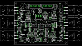
I guess a lot of people have done nice layouts of this amp. Here's my latest incarnation, with the triple output pairs.
Ten pounds of stuff in a five pound bag is what I call this crowded design, but it does fit in the max board size my freeware PC layout package will allow. They say 100x80mm, but that seems to apply only to pads. You can put bare board beyond that for mechanical clearance or support, which I did. I had to cheat and stand the power resistors vertically, that was my only option. Constructive criticism welcomed.
Ten pounds of stuff in a five pound bag is what I call this crowded design, but it does fit in the max board size my freeware PC layout package will allow. They say 100x80mm, but that seems to apply only to pads. You can put bare board beyond that for mechanical clearance or support, which I did. I had to cheat and stand the power resistors vertically, that was my only option. Constructive criticism welcomed.
Attachments
Hi Slowhands,
phew, I asked for it.
That is a sardines tin.
How many hours did it take?
This layout prompts the question.
How reliable is soldering power transistors into the wrong side of a single sided board?
phew, I asked for it.
That is a sardines tin.
How many hours did it take?
This layout prompts the question.
How reliable is soldering power transistors into the wrong side of a single sided board?
Hi slowhands,
Really nice compact layouts.
What components (if any) is off the PCB in the two layouts? I like the idea to be able to use 4 or 6 outputs on a boad of that size, it makes it easyer to find/make a suitable case and heatsink.
Hi Andew T,
I did make Rod Elliots P3A using his PCB, soldering the devices on the "wrong" side was no problem. You need to be carefull and make shure that there is no stress on the legs/pads when fastening the PCB and transistors or there might be a risk of lifting a pad (I did) easy to fix but annoying none the less.
Fasons might save you some space in place of the PC Power connectors. Just a thought. Easier too.
[EDIT] Nice job, btw!
[EDIT] Nice job, btw!
AndrewT said:...This layout prompts the question.
How reliable is soldering power transistors into the wrong side of a single sided board?
This is a double sided board with plated through holes and ample pads for soldering the output devices. It is slightly larger than 80x100mm, still about half the size of the original. It contains all components except the 6 output transistors, the 4 thermal sensing diodes, and the output Zobel network (R50/C25) which by design are mounted remotely.
This layout follows the Leach Amp design almost exactly, including using the same reference designators for all parts so that you can reference Dr. Leach's tutorials on the amp easily. To update this design to readily available plastic packaged output devices, the following enhancements were made:
- Added third output transistor and associated resistors; proven by many builders.
- 2N5415 parts changed to MJE350 and 2N3440 changed to MJE340; proven by many builders.
- Removed C19 and C20.
- Added optional input DC blocking cap.
- Added optional input ground resistor for ground loop reduction.
- Changed P1 to Multi turn cermet pot.
- 4 Fast rectifiers changed to ultrafast (that is, 1N4934 replaced by MUR120).
I do advise that the wiring of this system is critical if you wish to have optimal performance. You can introduce noise, distortion, or instability with a chance misguided choice of connecting or routing of wires.
This is because there is no such thing as "ground" in the real world. Every "ground" connection carries measurable current over a wire that has finite reactance that can be significant. Careful routing and twisting of cables is needed to minimize these effects. In particular, there are very high pulse currents flowing in the power and output wires that can radiate noise into the input wires or other circuits unless care is taken. These problems are very difficult to track down or observe, so it best to simply prevent them by using exquisite care in the wiring.
Central point grounding should be used in the wiring of this system. All wires labeled from the board labeled "Ground" should be returned separately to a single low impedance point connection, which I call "star ground". All wires from a connector should be twisted to ensure minimal coupling to other circuitry.
In particular the input ground and power ground must be returned separately to star ground, even though there is a connection between them on board (R51). The output ground wire is a shield, which returns to star ground (NOT to the speaker binding post ground). Note that the output Zobel network (of R50 and C25) is mounted on the speaker binding posts per Dr. Leach, and there is a SEPARATE ground return from the binding post ground return to star ground.
I use a copper buss bar between the main capacitor ground lugs for star ground. I drill holes in the buss bar, spaced equidistant from the cap ground terminals, for the star ground connections. I use a separate hole for the transformer center tap wire (which carries amazingly high alternating current pulses), a hole with a screw for power returns, and a separate hole for input returns.
If local law requires that the chassis be connected to safety "green wire" ground in the power cord, do so. It is my understanding that the USA and Canada so require. However, be cautious in adding a connection from star ground to chassis ground, as this is a prime noise source. Some makers have a switch to allow you to make this connection optionally, or to float the chassis. Other builders make this connection with an assortment of thermistors, resistors, bridges, capacitors and other circuit oddments. I leave that decision to the builder, personally preferring either no connection to chassis, or the switch. In a large system, floating is almost always best, but you should check.
In addition, all cables from connectors should be twisted for minimal noise coupling. This applies to the input wires, thermal diode wires, power wires, and output wires. The input wires and diode wires should be kept short, twisted, and routed away from the high current output and power wires. There is a ground wire with the output wires that is just a shield, and should run twisted with the output leads to the output binding posts, but not connect to a binding post; instead it returns to star ground. Again, there is a ground wire with the input wires that is just a shield, running twisted with the input wire but not connecting at the input jack; it returns to the star ground.
This may seem obsessive, but better safe than sorry.
That's all for now. Good day mates!
BrianDonegan said:Fasons might save you some space in place of the PC Power connectors. Just a thought. Easier too.
[EDIT] Nice job, btw!
Yes, they would save a little and I considered them. I went around and around on the choice of interconnects. What I ended up with does not fully please me, but I was somewhat limited in choices to what was in the library of the PC design program. All connectors are unique, polarized and multiply sourced (AMP and Molex, plus others). I wanted them to be idiot proof, because it would be easy to cook the amp by making a wrong connection, so I did not use Fast On connectors. You could simply solder wires to the holes too for the lowest cost and highest reliability. But on a proto, connectors are a must, so they stay for now.
One nice thing about the connectors you used is the pin spacing (5.08 if I remember correctly) allow for screw terminal blocks to be used as well.
- Status
- Not open for further replies.
- Home
- Amplifiers
- Solid State
- Smaller Leach Amp V1