Hi Jens,
I understand your reluctance to change a finalised PCB design at this late stage. The final decision is yours. I have a solution that can be retrofitted if needed. I am only trying to get the best for all the other Group Buyers.
Q. Any views on a slight delay in production to give Jens the time to try & find a solution to a potential deficiency?
Re post 259 - Power Supply decoupling.
The zener is a voltage reference and I believe the associated caps are there to lower the impedance and thereby minimise voltage variations appearing at the base of the cascode. These reference voltages do not have high current induced error signals on them from the output, driver or protection stages and so should not be introduced to that potential source of error.
The ground plane is what you will refer to as dirty.
So to sum up the parts that refer to signal ground on the original board:
Input LP filter (already implemented)
FB caps (already implemented)
Zener diode decoubling and zener diodes (missing at the moment)
Could some one please confirm this from the original board (I don't have one)
The ground plane is power ground
There are two connectiones on the board that allow the two grounds to meat at the central ground. There is a 10 ohm resistor between the two grounds on board.
\Jens
The power supply ground issue may not be as big an issue as presented by Self, since I just remembered the PS caps are on board. I haven't
The FB problem may have a compromise solution that would enable both options. Break the present trace between the emitter resistors and the feedback resistors, and provide vias to jumper between the vias to obtain the present state of board layout. Provide another via at the output to allow for an optional jumper from there back to the feedback resistor via. With a ground plane, the feedback jumper should present only a small loop WRT ground for either option.
The FB problem may have a compromise solution that would enable both options. Break the present trace between the emitter resistors and the feedback resistors, and provide vias to jumper between the vias to obtain the present state of board layout. Provide another via at the output to allow for an optional jumper from there back to the feedback resistor via. With a ground plane, the feedback jumper should present only a small loop WRT ground for either option.
I am in favor of the latter.
On the 10 device boards i am cutting the FB trace at R52, taking FB from the output back with a teflon insulated silver coax.
I did not bring this issue up previously as i am modding both circuits as is, and i am not keen on a separate FB-trace the way Andrew suggested, hope you dont hold it against me.
If a separate FB-trace on the board is required i'd add it on the bottom copper, centered, as short as possible.
(on my boards LSP return goes to the board, from there to PS ground)
Still the 10 transistor version, but new data to rewiev:
http://www.delta-audio.com/temp_jens/Leach_ver 6.7.10.zip
It's 1.6 Mb so take your time 🙂
Hopefully there will be no problems with reading the PDFs
\Jens
http://www.delta-audio.com/temp_jens/Leach_ver 6.7.10.zip
It's 1.6 Mb so take your time 🙂
Hopefully there will be no problems with reading the PDFs
\Jens
Bottom copper with the added trace looks good, imho.
You sure are fast with other things, Jens.
(Cool : "Layout by Jens Rasmussen")
After the trouble i had with the cable server i was thinking of stepping up to satellite.
btw: Never had trouble with the downloads from you, Jens.
You sure are fast with other things, Jens.
(Cool : "Layout by Jens Rasmussen")
After the trouble i had with the cable server i was thinking of stepping up to satellite.
btw: Never had trouble with the downloads from you, Jens.
Hey guys what are you talking about? I HAVE ONLY A DIAL UP 56K
line in my house, please, mercy, don't speak for speed
line in my house, please, mercy, don't speak for speed
To answer my own question about the ground on the original LEach PCB it looks like the ground to the zener diodes and their decoupling caps is in fact the power ground.
Look here: http://users.ece.gatech.edu/~mleach/lowtim/graphics/Compnt1.gif
\Jens
Look here: http://users.ece.gatech.edu/~mleach/lowtim/graphics/Compnt1.gif
\Jens
redesign leach pcb
Hi Jens, i think it is not a good idea to split the bottom groundplane in favor of not to solder a wire.
You are lowering the plane-impedance at the most powerfull part.
The idea as jacco did with a thin coax is much better imo.
I know the groundproblems from my earlier Leach design with a groundplane.
It is also important to isolate the pcb mounting screws from the chassis with nylon bolts or spacers.
I used 2 ground wires from that board: 1 from the groundside of the powersupply comps and one from the input circuit to star ground. Also 2 isolated RCA connectors.
Did you have groundloops with your pcb design as it is(was)?
Thanks, Loek
Hi,
I defer on the Zener ground. Keep it on the power ground if you're sure that's where it belongs.
Your summary of connections to signal ground sounds OK.
I like Pooge/Jacco's idea of pth conns for the NFB link.
I defer on the Zener ground. Keep it on the power ground if you're sure that's where it belongs.
Your summary of connections to signal ground sounds OK.
I like Pooge/Jacco's idea of pth conns for the NFB link.
Re: redesign leach pcb
Nope... And I don't really think the problem is loops... it's more like rectifier noise on the gnd that concerns Andrew..I think?
\Jens
loek said:Did you have groundloops with your pcb design as it is(was)?
Thanks, Loek
Nope... And I don't really think the problem is loops... it's more like rectifier noise on the gnd that concerns Andrew..I think?
\Jens
Regarding feedback
I have decided to leave the FB path the way I originally made it. I have provided an extra hole between R28+R30+D10+D12 to fit a feedback wire from the inside of the output inductor.
I have done this to maintain as much unbroken ground plane as possible, I hope everyone is ok with my choice, if not there is a chance to manually cut the FB trace and make the connection by means of a wire. If you cut the trace, be sure to make the FB connection before applying power to the amp, as there will be nothing to keep the amplifier output at 0 V DC.
\Jens
lowering the plane-impedance
I wrote lowering but you have to read worsening...
sorry for the mistake(hurry).
I am satisfied with the last modifications Jens.
Thanks again for your patience with last minute mods.
Loek
I wrote lowering but you have to read worsening...
sorry for the mistake(hurry).
I am satisfied with the last modifications Jens.
Thanks again for your patience with last minute mods.
Loek
JensRasmussen said:To answer my own question about the ground on the original LEach PCB it looks like the ground to the zener diodes and their decoupling caps is in fact the power ground.
Did you have the opportunity to measure SN on the 10-device boards, Jens ?
I have no equepment to perform S/N measurements.
I can just hear the amp at night with no music on there is a small hizz from the speakers when I put my head to the speaker.
\Jens
I can just hear the amp at night with no music on there is a small hizz from the speakers when I put my head to the speaker.
\Jens
Hi,
re post 273 - ground connections.
My concern was to keep the signal ground free from all/any contamination and to keep the feedback signal accurate.
Any contamination on these will enter the amplifier path & come out as mush, distortion, noise, intermodulation products from sub & supersonic signals & maybe some others that are equally unwanted & avoidable.
Jens, thanks for all your efforts.
Hello all.
I've studied hard the PCB this weekend and didn't see any major problems (ground loops etc).
Thanks Andrew for post 254, http://www.diyaudio.com/forums/showthread.php?postid=641411#post641411
Now, to go to the core of it.
I like what Jens has done with the new SG pin. Allso Jacco has a nice thing going with the shielded NF cable thingy.
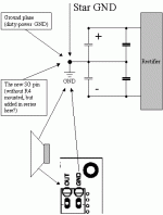
Afyer looking again at the board right now, i just came with this contraption (see attachment).
The ground plane around the input-vas stages does not have a great deal of current going around ( basically only C1 & C2 might drain some current through GND but that in the opposite direction, towards the power section) so no parasitic EM waves to disrupt the sensitive stages. And the voltage drop acros this GND section is too small (read allmost 0) to count on adding to the refference input voltage.
Therefore i thought of not mounting R4 on the PCB GND but instead use a shielded wire to the Master Star Ground with R4 inserted there. Both wires from this cable are tied together at MSG but only the inner conductor at SG.
Now this achieves (in my mind atleast) isolation between grounds.
Anyway, from my "meditations" it didn't had that much to gain over the current method (R4 on board).
Please put me to order on any thing i may have gotten wrong
I've studied hard the PCB this weekend and didn't see any major problems (ground loops etc).
Thanks Andrew for post 254, http://www.diyaudio.com/forums/showthread.php?postid=641411#post641411
Now, to go to the core of it.
I like what Jens has done with the new SG pin. Allso Jacco has a nice thing going with the shielded NF cable thingy.
Afyer looking again at the board right now, i just came with this contraption (see attachment).
The ground plane around the input-vas stages does not have a great deal of current going around ( basically only C1 & C2 might drain some current through GND but that in the opposite direction, towards the power section) so no parasitic EM waves to disrupt the sensitive stages. And the voltage drop acros this GND section is too small (read allmost 0) to count on adding to the refference input voltage.
Therefore i thought of not mounting R4 on the PCB GND but instead use a shielded wire to the Master Star Ground with R4 inserted there. Both wires from this cable are tied together at MSG but only the inner conductor at SG.
Now this achieves (in my mind atleast) isolation between grounds.
Anyway, from my "meditations" it didn't had that much to gain over the current method (R4 on board).
Please put me to order on any thing i may have gotten wrong
Attachments
Hi,
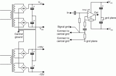
Regarding the layout…
Please don’t send anymore emails about payment yet… I will post information when I have finished the layout and then please acknowledge if you have something you need more information about.
Funny.... I just made this yesterday.
\Jens
Regarding the layout…
Please don’t send anymore emails about payment yet… I will post information when I have finished the layout and then please acknowledge if you have something you need more information about.
Funny.... I just made this yesterday.
\Jens
Attachments
- Status
- Not open for further replies.
- Home
- Amplifiers
- Solid State
- Smaller Leach Amp V1