
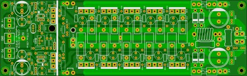
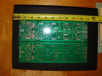
Look at the most recent layouts for the OPS. The current wisdom is more space and more even distribution for better thermal performance. I seriously doubt the 'old' layout is bad, it is just the idea that it can be done even better.
The precise post it is stated in is not remembered by me, but his latest design was meant to resolve that situation. He spread them out. AFAIK...
oh..... ok now I got it, maybe I can space them out a bit more, anyway I like the desisgn the way it is unless I just install 3 pairs and have spread them out I mean it might sound silly but is another way too to do it 🙂 if I don't want the full power of the 5 pairs installed
This will be fine using better cooling ,or mound 3 pairs out.tran.Look at the most recent layouts for the OPS. The current wisdom is more space and more even distribution for better thermal performance. I seriously doubt the 'old' layout is bad, it is just the idea that it can be done even better.
Last edited:
Can you share your Sprint File on that, I would like to add something to it. Thanks
I can later. It isn't complete yet, so what was it you had in mind to add?

Additional circuitry such as Caps and circuitry related to the 21st century protection thread. Yours would be a great starting point, and I would share it back once done.I can later. It isn't complete yet, so what was it you had in mind to add?
Jwilhelm already pointed out off-board to add the two pin connector for the protection board and the capacitance multipliers are part of the layout not yet shown. When I'm in front of my main computer I'll put up the file as it sits.
Additional circuitry such as Caps and circuitry related to the 21st century protection thread. Yours would be a great starting point, and I would share it back once done.

Jwilhelm already pointed out off-board to add the two pin connector for the protection board and the capacitance multipliers are part of the layout not yet shown. When I'm in front of my main computer I'll put up the file as it sits.
You should keep the exact spacing of the V2/V3 PCB's.
I,m stuffing a V3 now , lines up perfect with my V2 extrusion (even the Vbe).
V3 eliminates the 4 corner holes , as well. The outputs are all that is needed
to properly mount the board to the extrusion. 11 holes - that's it.
The only improvement that could possibly be made to the V3 is to
use C1/C2 layer parallel tracks and alternate the outputs (P/N/P/N/P).
Also - all the small diodes , 1/4w - 2w resistors ... everything -
I could bend the leads right to the body of the component (no lead
former - all hands). V3 is easier to build.
Edit- already have the 21'st century over-current integrated (will show a complete V3 soon)
OS
Hi OS,
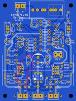
I redrawing Symetri under Diptrace. I don't know if it is a mistake but i found a difference between schematic and layout => C9 (R33 if we follow straigh the schematic) should be connected to Q8 collector and C33 but not to Q8 base
I redrawing Symetri under Diptrace. I don't know if it is a mistake but i found a difference between schematic and layout => C9 (R33 if we follow straigh the schematic) should be connected to Q8 collector and C33 but not to Q8 base
Attachments

You should keep the exact spacing of the V2/V3 PCB's.
I,m stuffing a V3 now , lines up perfect with my V2 extrusion (even the Vbe).
V3 eliminates the 4 corner holes , as well. The outputs are all that is needed
to properly mount the board to the extrusion. 11 holes - that's it.
The only improvement that could possibly be made to the V3 is to
use C1/C2 layer parallel tracks and alternate the outputs (P/N/P/N/P).
Also - all the small diodes , 1/4w - 2w resistors ... everything -
I could bend the leads right to the body of the component (no lead
former - all hands). V3 is easier to build.
Edit- already have the 21'st century over-current integrated (will show a complete V3 soon)
OS
OS, I get where you are coming from. When I started that version of the artwork I didn't really give much consideration to a V2 'upgrade' path. I don't think there is so much wrong with V2 that those who have built already would need or want to replace V2 with whatever should follow it. That said I wanted to incorporate some of the newer thinking with a few ideas of my own.
When it comes to resistor / diode pad spacing I try to leave a little extra space as I always understood it was somehow bad to bend a components leads right against the body. That also leaves a little wiggle room for different brands or series to fit as well since we are all likely to source parts differently.
The staggering of N and P may be a bit of added refinement, but to what real-world benefit? Better thermals and some field cancellation would be just about it. Especially with odd numbers of output pairs.
One thing I would like to consider is putting the drivers on the main heat sink and using the compound Vbe to monitor the pre-drivers and run the whole driver / pre-driver setup a little harder. Any thoughts on that? In the simulator the extra current in the pre-driver / driver stages helps with stability, along with a little resistance directly in the collector circuits of the drivers and pre-drivers.
While I'm always open to ideas , the present H/K Vbe is superior.
Say you are driving a given "light" load ... all of a sudden your load
increases X4.
What will happen ?
First your outputs Ie/Ib will increase X4 , driver dissipation will increase the same.
The small driver heatsink will heat up rather quickly , changing the
output Vbe in seconds. Just a Vbe on the output stage would take 10's
of seconds to respond to the same increased demand.
H/K kept this same Vbe from 1980's almost until 2005 (HK 990). ALL the
integrated amps and receivers up to this date have the best of reviews.
The logical "better" Vbe would be the 990 approach , have one pair
of the outputs with a integrated die diode (thermaltrak) , and change
the Vbe Tc in milliseconds instead of seconds.
PS - most leave the predrivers alone. Even if your ran them much "hotter"
they would not have much effect on Tc.
OS
Last edited:
Hi OS,
I redrawing Symetri under Diptrace. I don't know if it is a mistake but i found a difference between schematic and layout => C9 (R33 if we follow straigh the schematic) should be connected to Q8 collector and C33 but not to Q8 base
I see what you mean. Amazing the circuit worked as I built it. Please see attached. I moved things around a bit. I think I have it corrected.
Blessings, Terry
Attachments
jkuetemann,
If you look at some old military specs they would never allow straight bending of the leads straight down against the body like that, they always show a bend radius, it just makes sure you never have a failure due to a cracked lead over time. Today I don't know as most things are going surface mount but I would assume for thru hole applications that would still hold true.
If you look at some old military specs they would never allow straight bending of the leads straight down against the body like that, they always show a bend radius, it just makes sure you never have a failure due to a cracked lead over time. Today I don't know as most things are going surface mount but I would assume for thru hole applications that would still hold true.
- Home
- Amplifiers
- Solid State
- Slewmaster - CFA vs. VFA "Rumble"