OS,
Your LTSpice simulation commands do not have a long enough delay for the power supply voltages to settle. For those keeping score, this affects THD data.
==========
Elaborate ,I will throw anything into the simulations to "cripple them"..
PS -I also put inductance' s and resistance's into the rails to try to simulate "real world"
performance. No "ideal" sources used ! I usually come very close to the real thing.
OS
Last edited:
i follow your work,and i have your mongrel amplifier done by nikko,sounds...well sounds so well that it made me read whole "mogrel" thread and extract all files out of it 🙂 since some say that it came out of sym-asym,that one is in your folder too 🙂
i also like the way you do it - modular way,great idea!
than came the honeybadger,the thread taht i somehow totaly missed,and now this one. well,now you have your own folder im my "elektronika" folder. you are doing a great job here,and it looks so easy when i see you doing it. in a just few weeks from basic idea to a few working versions.
thank you man!
Attachments


Os,
Where is the CFA FE for your standalone triple output stage? Gonna give it a try.
A few posts back - it is the "Slew-NADH-v1.1.zip"
OS
i follow your work,and i have your mongrel amplifier done by nikko,sounds...well sounds so well that it made me read whole "mogrel" thread and extract all files out of it 🙂 since some say that it came out of sym-asym,that one is in your folder too 🙂
i also like the way you do it - modular way,great idea!
than came the honeybadger,the thread taht i somehow totaly missed,and now this one. well,now you have your own folder im my "elektronika" folder. you are doing a great job here,and it looks so easy when i see you doing it. in a just few weeks from basic idea to a few working versions.
thank you man!
Thank you , I will continue to innovate 🙂 .
OS
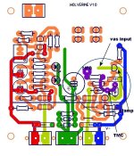
Wolverine is evolving ...
Put to the CAD , the layout is immaculate (below).
On the smaller 75mm X 75mm standard - plenty of room to be
"anal" 😀 .
Each section of the amp has it's own "real estate" , CCS's together
share the positive side of the layout -VAS the negative.
Below the VAS heatsink , all sensitive TMC (compensation) components will be
very close to the VAS (B-C) .
With these IPS's , the full OPS signal will be brought right to the board ...
so the NFB pad will be further away from the LTP + "guarded" by ground traces.
This means the DC cap , and the FB divider will also have a separate piece
of "real estate" separated by several mm's from either the mirror or LTP.
The "wolverine" should run in the same pack with cousin Badger. 😀
OS
Attachments
Last edited:
Member
Joined 2009
Paid Member
Brother sucks ... they say.
I can confirm that. I have a Brother laser at home and it doesn't work at all for Toner Transfer pcb making. The problem is that it creates a transfer with poor coverage, it's thin and patchy and inadequate for the job. It's as if it is designed to use the least possible toner, for home use, even if you select 'darker'.
I use a glossy magazine with a lot of clay content.
This is my experience too - works well. But one thing that I found was key to good results and it surprised me - do not iron the pattern onto the board, but iron the board onto the pattern. I found best results when I put the magazine paper with toner on it face up on a sturdy bench. Then place the pcb copper-layer face down onto the paper. Then iron the back of the board - with a fair bit of downward pressure. I remember I was about to give up altogether, it was my first project and I was new to the forum - only when I tried having the board over the paper did I finally get it to work well. I think ironing the board helps because it makes the pressure and the heat more uniform.
i like the plan, finally a chance to make two amps, one CFA and one VFA with identical output stage
I already have PCB's in hand for such a beast - the TGM7. I haven't had time to build the CFA version, the VFA is up and running. I'm hoping 'Pinnocchio' will be able to help out - I sent a pair of boards recently. It has both variants on a single pcb with very very few differences between the CFA and VFA versions. Once I have built it I'll let you know what I 'hear' - I assume the more the merrier when it comes to collecting our experience on this topic.
Last edited:
I already have PCB's in hand for such a beast - the TGM7. I haven't had time to build the CFA version, the VFA is up and running. I'm hoping 'Pinnocchio' will be able to help out - I sent a pair of boards recently. It has both variants on a single pcb with very very few differences between the CFA and VFA versions. Once I have built it I'll let you know what I 'hear' - I assume the more the merrier when it comes to collecting our experience on this topic.
TGM- xx IPS's ??? Would you give me permission for "tweaking" to "slew"
specs ? (<20ma +/- rail demand and 4-5ma VAS I).
OS
Member
Joined 2009
Paid Member
I'm not sure what you're asking but I'd welcome any interest in my project - so knock yourself out!
This isn't a ground-up design by my own brain - I started with Greg's SKA which is VFA. So it will have deficiencies as it was never intended to be an optimal CFA. I also got some inspiration from 'Fab' who had the same idea more or less. What I've made in terms of a CFA is simple, akin to the Pass F5 in some ways. The IPS is a complimentary pair of Singletons which feed into an EF buffered VAS. The VAS is the output. It has atrocious PSRR but this is the price paid for it being 'too simple'. In VFA form it is already a 'fast' amp and so far my impressions of the sound are very positive.
http://www.diyaudio.com/forums/solid-state/239418-tgm7-amplifier-based-greg-ball-ska-5.html
Put to the CAD , the layout is immaculate (below).
On the smaller 75mm X 75mm standard - plenty of room to be
"anal" 😀 .
Each section of the amp has it's own "real estate" , CCS's together
share the positive side of the layout -VAS the negative.
Below the VAS heatsink , all sensitive TMC (compensation) components will be
very close to the VAS (B-C) .
With these IPS's , the full OPS signal will be brought right to the board ...
so the NFB pad will be further away from the LTP + "guarded" by ground traces.
This means the DC cap , and the FB divider will also have a separate piece
of "real estate" separated by several mm's from either the mirror or LTP.
The "wolverine" should run in the same pack with cousin Badger. 😀
OS
what i like in OS designs is that they are mostly single sided so that a diyer making his own boards can do so easily...
i am old and hands are not as steady as when i was younger so that OS boards are very doable for me....😀
I already have PCB's in hand for such a beast - the TGM7. I haven't had time to build the CFA version, the VFA is up and running. I'm hoping 'Pinnocchio' will be able to help out - I sent a pair of boards recently. It has both variants on a single pcb with very very few differences between the CFA and VFA versions. Once I have built it I'll let you know what I 'hear' - I assume the more the merrier when it comes to collecting our experience on this topic.
thanks for the heads up, i got involved in the badgers when someone bought all parts and gave them to me to build for him, i am hooked...
i am sure your project your project is likewise good, just that smd scares me at the moment...😀
thanks for the heads up, i got involved in the badgers when someone bought all parts and gave them to me to build for him, i am hooked...
i am sure your project your project is likewise good, just that smd scares me at the moment...😀
Join the "club" !! No $$ here- (wife takes that).
Have 3 toriods of 25-0-25v to
35-0-35v that I "rescued" from E-waste. I also have almost 100KG of copper wire,
....that will be my next mouser order $$.
I order scrap FR-4 off of ebay from a vermont dealer.
I will order the OEM toner cartridge from HP (it is the best).
So ... I design from the "crevasse" (always looking up) 😀.
My designs will turn partial E-waste into SOTA designs.
OS
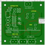
Wolverine "fine tuning" ...
The VAS and the TMC compensation is the "foundation" of the famous
"blameless sound".
The layout is crucial ... since the main pole of the amplifier is determined
here , short traces and "compactness" is required.
(below) .. The 2 silver mica caps are VERY close to the beta enhancement
and main VAS device . The feedback resistor from NFB to TMC is also
VERY close. A long trace here would possibly add parasitic C to the "mix".
On the "wolverine" , a saturation clamp is also employed. It's traces are
also " anally" short ... as it is a "full partner " in this close tolerance
section of the amplifier.
Now , we are down to the LPT/CM ... No issue here , just separate it
with a couple centimeters of board space and run direct V- to the CM Re's.
The LTP is "set" with the "badger style" 2.2K resistor from the small
CCS.
Input will be standard fare ... referenced to the lifted ground (green traces).
This will be the most fault tolerant of the "blameless'es" , able to
even allow for 1.5mhz unity gain operation with VERY good 78 degrree
margin (super stable - below 2). In the simulation I used 220p/47p/1.5K for the TMC.
All this with E-waste or $.30-.70c mouser semi's.
VFA - VFA - VFA ..... Let me hear a - VFA !!! 😀😀
OS
Attachments
Last edited:
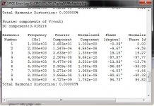
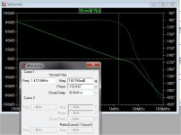
Broke the "record" with this one.
1Khz nearly full power - 3R load (below).
Doug Self would be proud ...
PS - I suppose that's why it is "blameless" ?? 😀
OS
I have a question if I may, and its over how much confidence you can have in all of these results (generally, I'm not just singling this one out) ?
My reason for asking is this. Manufacturers of small signal opamps (vfb I know but the principle must hold true) always state in the data sheets that the distortion of 0.0000xxx of a particular device is below the measurable limits of any available measurement equipment. To get a real measurement the distortion has to be artificially raised by manipulation of noise gain (let the amp amplify its own distortion). Only then can the amp as a whole be measured and and a distortion figure arrived at. That all has to be done on a real device, not a simulation.
Does component matching play a big part here ? In the simulator all semiconductors (and all like parts come to that) are carbon copies of each other. If you hand matched real devices you would be lucky to get within a few percent of a perfect match. I've often thought it would be a good idea to have a set of devices in simulation that were "the same" but "different" by perhaps 5 or 10% in various parameters. When you sim a design you randomly pick from a list of say 10 possible versions, each "the same" within say the 10% figure of a reference device of that type.
Here you seemingly have power amps offering figures that on the face of it are truly remarkable (and then some) considering they are delivering serious power to a low impedance load.
The killer question and proof of all these is whether anyone with access to equipment capable of distortion analysis has actually tested one of these designs and seen how it compares to the sim.
No special matching , in fact ... once you reach a "sweet spot" in the bias
of the CM/LTP/VAS , this particular design does the rest.
The layout of the PCB is the final key to approaching what the simulator
tells us.
I do "cripple" the simulations slightly with C/R/L. A mismatch in the CM/LTP
would give me mid - double digit PPM (30-50) ..A VAS-OPS mismatch would
only affect offset.
So , I you used a curve tracer on the LTP/CM devices ..
I would say you could come REAL close to sub PPM with this design.
A hefty power supply
would also allow for PPM into high power.
Electrically , I have simulated countless real amps (for repair/troubleshooting)
... the models/simulations are within percent(s) of the real amps.
Shorting out one device on the simulation will tell me what other devices are overcurrent ...
and "fried" (did this on the "badger build thread").
It is just a very powerful "tool" .... same as a DMM/scope/iron 🙂 .
OS
Broke the "record" with this one.
1Khz nearly full power - 3R load (below).
Doug Self would be proud ...
PS - I suppose that's why it is "blameless" ?? 😀
OS
Very good, what on 20k?
No special matching , in fact ... once you reach a "sweet spot" in the bias
of the CM/LTP/VAS , this particular design does the rest.
The layout of the PCB is the final key to approaching what the simulator
tells us.
I do "cripple" the simulations slightly with C/R/L. A mismatch in the CM/LTP
would give me mid - double digit PPM (30-50) ..A VAS-OPS mismatch would
only affect offset.
So , I you used a curve tracer on the LTP/CM devices ..
I would say you could come REAL close to sub PPM with this design.
A hefty power supply
would also allow for PPM into high power.
Electrically , I have simulated countless real amps (for repair/troubleshooting)
... the models/simulations are within percent(s) of the real amps.
Shorting out one device on the simulation will tell me what other devices are overcurrent ...
and "fried" (did this on the "badger build thread").
It is just a very powerful "tool" .... same as a DMM/scope/iron 🙂 .
OS
Thanks OS. Sounds like you have confidence in the basic design... and thats good. Layout is everything, absolutely no argument on that front.
Interesting to hear your practical experience of real vs sim on some actual "real" designs. My nagging doubt is that an amp of (say) 0.01% thd could well perform pretty much like the sim. An amp of 0.001 perhaps less so but still close, but when you get to 0.000005%, well you see where I'm coming from. If the distortion of the real thing was a 1000 times worse it would still be a pretty remarkable amplifier.
So at some point (to my way of thinking) this needs an amp of this topology submitting for real and detailed measurement to see what the reality really is is.
Anyhow, thanks for sharing your thoughts...
OS do you mind sharing the "blameless" ips and ef3 output, ltspice .asc file.
It would help me alot, I still have very much to learn 🙂
Regards
It would help me alot, I still have very much to learn 🙂
Regards
TGM- xx IPS's ??? Would you give me permission for "tweaking" to "slew"
specs ? (<20ma +/- rail demand and 4-5ma VAS I).
OS
Ostripper, If you have time please look IPS of The Ampz Pages - the DPA 220. It have nice clipping behavior. Can you optimize the IPS?
I simulating your DIYA amp, but I have nasty clipping behavior at one side of power supply.
- Home
- Amplifiers
- Solid State
- Slewmaster - CFA vs. VFA "Rumble"