
Yeah, it's hard to get a good angle on it bc when it was built in factory , it's sitting at a slant. And slanted w/ it facing Face Down. Which makes it even harder to do anything w/ it. I'll take pics facing down . Or at least try. I can send em around lunch time. Thank you sir! !

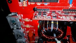
I don't understand what you're trying to show from the edge of the board. The traces are on the face of the board. The transistors don't show Q12 (which is what you said that you had the problem with).
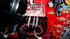
Well, as I mentioned in the earlier posts, why are the driver board bent in like that? And it won't let me load other pics? Says missing token???

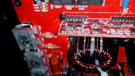
The transistors are supposed to be MMBTA42s and MMBTA92s. It appears that you have 2N7002s installed.
The holes in the board may have allowed the board to tilt before soldering. It's also possible that the connector is bent. Sometimes they lean as far back as your leans forward.
The holes in the board may have allowed the board to tilt before soldering. It's also possible that the connector is bent. Sometimes they lean as far back as your leans forward.
Perry,
I ordered the right ones yesterday, must had a typo when ordering the 1st time. So on the bent driver board, can I warm up the solder and try to realign it straight, so it's easier to work on?
I ordered the right ones yesterday, must had a typo when ordering the 1st time. So on the bent driver board, can I warm up the solder and try to realign it straight, so it's easier to work on?
If you remove the end plate and stand the amp on end, you should be able to do it like it is. Trying to straighten it may cause more problems.
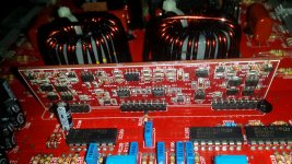
While you have the transistors off, take a photo of the traces for the each transistor so you can make jumpers if you break a pad.
When you solder the new transistors on, clean all of the original pads of all solder with desoldering braid and then remove the flux with alcohol or acetone. Let dry and apply a very small amount of solder to an easily accessible pad. Place the transistor in place and apply pressure by squeezing the transistor and the board together with tweezers. That will prevent it from moving. Touch the iron to the terminal on the pad with solder to melt the terminal into the solder. Then solder the other pads.
Yeah I will unmount it before working on it. It's still ackward working on it bc you think your working on a flat surface, but really it's slanted. How would I make a trace? I framed out big time when the little square pad came off with the solder!! Looked like it was just glued to the board. Do they make replacement? Or?? And I have a Skar 1500.1 amp too , doing same thing but it starts out at 13.84 volts then looses voltage down to 7/8V?? Any common issues with this model? It's half the size of the T1400.1 , figured I'd start on this one till the new transistors get here either on Tues or Wed.
P.S. Just wanted to stop and say thank you for your time and help on this amp.
P.S. Just wanted to stop and say thank you for your time and help on this amp.
Stand the amp up so that the board you're working on is a level surface.
You don't replace the printed trace. You use a small wire, like that from a computer ribbon cable to connect across the broken trace. That's why I want you to photograph the traces under the transistors when you have them off of the board.
Don't mix amp repairs in a thread.
You don't replace the printed trace. You use a small wire, like that from a computer ribbon cable to connect across the broken trace. That's why I want you to photograph the traces under the transistors when you have them off of the board.
Don't mix amp repairs in a thread.
I had to use jumpers to repair a driver board where the transistors burned through some of the original traces. There is one jumper from collector to collector. Another from emitter to emitter and one on the edge of the board that connects the two NPN collectors to the positive supply. Your will be different if you need to repair any damaged/missing pads/traces. This is simply an example.
Adhesive will be applied to various points to ensure that nothing breaks loose.
Adhesive will be applied to various points to ensure that nothing breaks loose.
Attachments
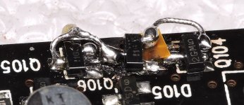
Ok Perry, I got the new transistors yesterday. Part of that pad was still on there, it just got turned some how. This driver board reads good now, but input rail only reads on middle leg on all of them.. did I screw something up when I had the wrong size transistors on driver board? I can take pics of 2nd driver board. Or do you have any other ideas of what it might be sir?

I also have a question that no one can give me a simple answer without making my head hurt n comprehend. How can I tell the difference between regular diode and a zener diode, I think I spelled it right?? Lol. Hard to tell with only them using 3 to 4 letters or numbers on the actual component?
What do you mean by:
but input rail only reads on middle leg on all of them
Most diodes are marked. For those that are not, you have to look at the circuit to try to determine what they are. Which ones are you trying to identify? What is the marking on it?
but input rail only reads on middle leg on all of them
Most diodes are marked. For those that are not, you have to look at the circuit to try to determine what they are. Which ones are you trying to identify? What is the marking on it?
- Status
- Not open for further replies.
- Home
- General Interest
- Car Audio
- Skar Audio T1400.1 protection light flashes fast on/off?