just a note of caution when mounting R6
do not mount it on C4 pads
edit ... board survived removing the R6, but resistor didn't
gosh, this is almost like having hangovers 😱😀
do not mount it on C4 pads
edit ... board survived removing the R6, but resistor didn't
gosh, this is almost like having hangovers 😱😀
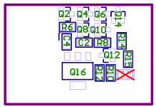
all resistors mounted (except R1,2,3,4)
another one 'jumped over board' ... luckily I had a spare
another one 'jumped over board' ... luckily I had a spare
I see that I have forgot to mention those in my description but if your connection is permanent and DC connected to the source you don't need pullup/pulldown resistors at all but in case you have a potentiometer, having a coupling cap or if the input can be disconnected the bias currents need a path to other ground or the supply rails. You will need one resistor if you have a dual power supply and two resistors if you have a single supply.
I understand
read you said this before
but you have crossed R3 (post#143)
is new board layout is different ?
(schematic shows input pulldown res as R1)
😕
read you said this before
but you have crossed R3 (post#143)
is new board layout is different ?
(schematic shows input pulldown res as R1)
😕
I will make this more clear but the main thing is that you always have a path from the input to somewhere you can get a base current, if not you can have a nasty offset at the output. The documentation says R1 and not R2 and R3. I case you had special needs I added one extra 1 Mohm in the kits.I understand
read you said this before
but you have crossed R3 (post#143)
is new board layout is different ?
(schematic shows input pulldown res as R1)
😕
A trick is to put very little tin on one pad and then place the part and melt the tin. Atfter that solder the other pad normally.gosh, this is very difficult
and lost half of one solder pad(maybe two)
components look 'well cooked' 😱
and probably worse than it looks 😀
I will feel lucky if it works 🙂
A trick is to put very little tin on one pad and then place the part and melt the tin. Atfter that solder the other pad normally.
that is exactly what I do 🙂 holding down with a tool in right hand, and solder iron in left hand 😀 all while looking through a magnifier glass 😱
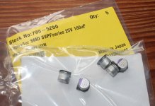
got 10 small lytics today 🙂 and hopefully correct size this time 
http://docs-europe.electrocomponents.com/webdocs/1251/0900766b81251945.pdf
3200mA and 24m ohm(0.024) ... that is impressive
http://docs-europe.electrocomponents.com/webdocs/1251/0900766b81251945.pdf
3200mA and 24m ohm(0.024) ... that is impressive
Attachments
I just noticed when going through the documentation that the circuit can use also lower operating voltages than +/-15V. Is there any downside to use for example +/- 9V or +/- 12V instead of that 15V nominal?
Erm. No news regarding buffers. Finished to build QRV09 recently, working fine with HD650 🙂 No buffer needed 🙂
Unfortunately no news about the buffers. I have been concentrating on other projects lately, namely those which do not need a soldering iron as mine failed. When I get a new one, then I'll continue with the buffers as well.
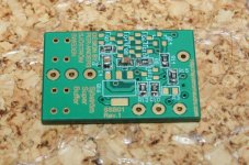
My 4 buffer are soldered and tested ... also I finish one SSR03 power supply ... and I'm very satisfied with results especially with SSR03
Thanks for this great projects
Thanks for this great projects
- Status
- Not open for further replies.
- Home
- Group Buys
- Sjöström Diamond Buffer group buy