Hello all
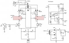
I have built a circlotron power buffer using 2SK82 as an experiment.
To know the sound characteristic of power device, this type of simple push-pull balance buffer is the choice, I think.
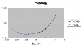
I attached entire circuit and measured distortion data. The bias current is set to 0.5A per SIT.
I have built a circlotron power buffer using 2SK82 as an experiment.
To know the sound characteristic of power device, this type of simple push-pull balance buffer is the choice, I think.
I attached entire circuit and measured distortion data. The bias current is set to 0.5A per SIT.
Attachments
This is a very interesting design thank you for posting.
After some studies and thinking about your choices, I will ask some questions ....
After some studies and thinking about your choices, I will ask some questions ....
Kasey197 and Nelson,I think that's very nice, but I would be inclined to regulate the bias voltage
as well.
😎
thank you very much for your comment.
I plan to regulate the bias with TL431A voltage multiplier shortly.
I additionally show you the mounting of the regulators.
This method can reduce ESL and ESR of wirings and also make the power block very compact. As the regulator is LDO, generated heat is few watt even at full power load and thus collocation is OK.
This power block dissipates 25W at idle state.
Attachments

now become a balanced power amplifier.
Hi.
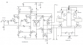
This CSPP (or Circlotron) power buffer has a differential preamp stage and becomes a balanced power amplifier now. The VAS I developed is a discrete fully differential amplifier (FDA) with no feedback and enable this FDA differential outputs directly connect to the SIT gates the level is the bias voltage of SIT and around -10V.
I also provide DC detection and power shutdown scheme to prevent very rare 2SK82s from destroy.
The sound? Vivid and clear!
Hi.
This CSPP (or Circlotron) power buffer has a differential preamp stage and becomes a balanced power amplifier now. The VAS I developed is a discrete fully differential amplifier (FDA) with no feedback and enable this FDA differential outputs directly connect to the SIT gates the level is the bias voltage of SIT and around -10V.
I also provide DC detection and power shutdown scheme to prevent very rare 2SK82s from destroy.
The sound? Vivid and clear!
Attachments

Hi Gantez,
Very nice,like to make one.Have some questions.
Can I use 2sk60 ( small power) or 2sk180 (for higher power) as the direct replacement of 2sk82 without any modification? or 2sj28 with modification (output voltage polarity reversal)
Can you publish complete schematics including protection circuits,power supply for small signal stage,biasing etc?
what is ATT h and ATT c? Is it goes to protection circuit?
Picture shows two small tranformers,what is the use of second one? first one I know?🙂
Thank you very much for sharing Ideas
Best regards
Joshvi
Hi Gantez,
Can I use 2sk60 ( small power) or 2sk180 (for higher power) as the direct replacement of 2sk82 without any modification? or 2sj28 with modification (output voltage polarity reversal)
Can you publish complete schematics including protection circuits,power supply for small signal stage,biasing etc?
what is ATT h and ATT c? Is it goes to protection circuit?
Picture shows two small tranformers,what is the use of second one? first one I know?🙂
Thank you very much for sharing Ideas
Best regards
Joshvi
Hi Joshvi.
I belive replacement with 2SK60 and 2SJ20 is quite easy as you mentioned.
But replacing with bigger 2SK180 , you need to add a buffer to drive bigger equivalent input capacitance. Otherwise high cut off frequency will fall down into audio frequency range. A complementary BJT buffer will solve this issue.
ATT H and ATT C are the connector for a step shunt attenuator which has switched resistors. Because this VAS is current output, changing load resistor makes the output level proportional to the resistance.
This type of post attenuation can improve signal noise ratio and reduce drift degraded by VAS and interestingly reducing output impedance.
When this ATT level is in the middle and say -20db(1/10), the high cut F is 10 times larger.
One of the transformer is very important and always on, this is for SIT bias and offset protector, the other transformer is switched and for for VAS dual PS.
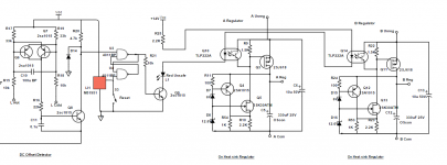
Here is other circuits with short description.
1.AC input, VAS DC supply and Shunt ATT
In the middle, unfamiliar power supply uses simulated inductor; gyrator to form a virtual CLC filter. LED and diodes reduces drop out by pass MOS transistors.
This LDO gyrator is my original.
The center of this PSU is NOT connected to ground but -Bias L to maximize VAS output swing.
2. Bias and logic supply
Regulated OPS bias is generated here by TL431 and becomes the center level of VAS PS and the VAS differential output reference also.
3. Balanced DC offset detector, the latch and shutdown and also two floating OPS regulator .
Original balanced DC offset detector always monitor DC level at the speaker terminal. If DC present、set the latch , shutdown OPS voltage until reset by switch or AC disconnect and lit on-board red LED .
This circuit is dedicated to each channel and makes easier to find faulty channel.
Attachments


Lot of interesting ideas like shunt att. and LDO gyrator.
2sk82 is very difficult to get. so I like to use 2sj28.Is the main supply polarity reversal will do the trick? Is required any modification to VAS stage?
Thankyou
Best Regards
Joshvi
2sk82 is very difficult to get. so I like to use 2sj28.Is the main supply polarity reversal will do the trick? Is required any modification to VAS stage?
Thankyou
Best Regards
Joshvi
thanks for sharing...i have 11 2sk82es , used but still working...
How about parts..can we substitute others parts that are not available like 2sj618,k2925, TJ11A10m3...
Can we replace those with similar or close equivalent mosfets?
How about parts..can we substitute others parts that are not available like 2sj618,k2925, TJ11A10m3...
Can we replace those with similar or close equivalent mosfets?
Hi.
This CSPP (or Circlotron) power buffer has a differential preamp stage and becomes a balanced power amplifier now. The VAS I developed is a discrete fully differential amplifier (FDA) with no feedback and enable this FDA differential outputs directly connect to the SIT gates the level is the bias voltage of SIT and around -10V.
I also provide DC detection and power shutdown scheme to prevent very rare 2SK82s from destroy.
The sound? Vivid and clear!
One should not forget about relatively high output impedance of such a buffer, I guess few Ohms. Not quite good for real world speakers.
I was thinking about bridged output buffer with power VHF bjt transistors, 4A+4A or even higher idle current. Hope to get 0,2...0,3 Ohms output impedance.
One should not forget about relatively high output impedance of such a buffer, I guess few Ohms. Not quite good for real world speakers.
I was thinking about bridged output buffer with power VHF bjt transistors, 4A+4A or even higher idle current. Hope to get 0,2...0,3 Ohms output impedance.
VladimirK thank you for your comment. Dumping Factor is one of the important parameter of modern amplifier which needs to drive low effficiency modern speakers. The output impedance of this amp might be around few ohms because the 2SK82 Rd is around 10 ohms. But when you listen to tube amps which has low DF, sounds good and comfortable. I would like to reproduce tube like but more wide range sound from this amplifier. I have driven many kind of speakers, my TAD TM1201 100db/w backloaded 3way horn system ,JBL twin 15" front loaded horn 3 Way system and Kenwood 15cm 2way system and felt vividness from them.
Lot of interesting ideas like shunt att. and LDO gyrator.
2sk82 is very difficult to get. so I like to use 2sj28.Is the main supply polarity reversal will do the trick? Is required any modification to VAS stage?
Thankyou
Best Regards
Joshvi
As the polarity is opposite, you need to revers drain voltage to negative and the gate bias voltage to positive. And the bias is connected to VAS output common and also to VAS DC center, it is OK.
VAS stage R14,2.2K and R32, 2.2K are required to be removed for keeping first stage foot(?) room.
thanks for sharing...i have 11 2sk82es , used but still working...
How about parts..can we substitute others parts that are not available like 2sj618,k2925, TJ11A10m3...
Can we replace those with similar or close equivalent mosfets?
Junm, You have many 2SK82! I envy you.
These all are in DC power line so the most important characteristics are Vdss and Id max. and also Y(gm) , audio grade device is not necessary but robustness is the key. It is better to avoid far bigger device which has big inter electrode capacitance and thus degrades high frequency performance of these circuit.
Very interesting.Clever ideas.I understood why R14 and R32 is removed or decreased.But in VAS psu schematic both bias supply and ground is connected to centre point by mistake.
Best Regards
Joshvi
Best Regards
Joshvi
Sorry I mean 2sk182 es...the big one....but i have a lot of 2sk60 and 2sj18 around 20 pairs most of them rank 4. I can parallel as many as required.Junm, You have many 2SK82! I envy you.
These all are in DC power line so the most important characteristics are Vdss and Id max. and also Y(gm) , audio grade device is not necessary but robustness is the key. It is better to avoid far bigger device which has big inter electrode capacitance and thus degrades high frequency performance of these circuit.
Very interesting.Clever ideas.I understood why R14 and R32 is removed or decreased.But in VAS psu schematic both bias supply and ground is connected to centre point by mistake.
Best Regards
Joshvi
I use different symbols for chassis ground, digital ground and Analog ground.
the VAS supply connected to this Analog ground and also it's bias level. This might confuse you. so please forget this analog ground.
The VAS supply is +/-30 volt from their center. But when you built into this amp, Bias shift -10V is applied to the center, so measuring the voltage from chassis, they are now become +20V and -40V.
As input front end works at this level, you need to care the voltage and heat caused by this bias shift.
Thus I put voltage dropper to input CCS.
When I consider 2SJ28 OPS again. the apparent VAS supply voltage now becomes -20V and +40V. And , this +40V is quite big for small signal transistors. Avoiding this by voltage dropper does not works well this time. Cascode might be the solution to this VAS amp but 2 serial cascode is too many.
A Complete solution to this issue I think is to build opposite polarity VAS board that has completely swapped NPN to PNP, NJFET to PJFET and PNP to NPN and with voltage dropper.
From post 7,first two schematics VAS PSU and Bias PSU centre points are connected to digital ground.This will short circuit the bias supply.Yes,removing the digital ground from VAS PSU will solve this.
I know you designed this circuit as circlotron buffer,but what will happen if i connect the load between VFETs drain instead of sources.I am not much familiar with circlotron.
Thank you
Joshvi
I know you designed this circuit as circlotron buffer,but what will happen if i connect the load between VFETs drain instead of sources.I am not much familiar with circlotron.
Thank you
Joshvi
I know you designed this circuit as circlotron buffer,but what will happen if i connect the load between VFETs drain instead of sources.I am not much familiar with circlotron.
Thank you
Joshvi
You see each drain is connected to buddy's source by floating supply which is considered as short in ACwise.
Therefore, the load between drains receives the same AC signal as that of load between sources. Only difference is the DC voltage level.
- Status
- Not open for further replies.
- Home
- Amplifiers
- Solid State
- SIT 2SK82 Circlotron Power Buffer