@pras1170,
they are arrived, thanks! 🙂
But the customs had taken additional fees (40€). :-(
An externally hosted image should be here but it was not working when we last tested it.
Germany is customs expensive, bääääh!
God, such a high customs fee, it is still sending CHINA POST, there should be no tariffs (I declare a very low price, the result will be charged tariff)
DHL, declared a real transaction amount is: USD 3080 The result does not require any fees, the customs release, no need to pay
In some countries, it may be very strict, so it leads to customs fees.
I am very sorry this time, you have spent a lot of customs duties.

Yepp you did edit it. Not nice [emoji6] and not right! I had found these two on my own, but none showed the pin naming in another language than Japanese. So I asked. So I was right, stupid but not lazy. Other way round would be smarter...
Don't take me too serious. I should have added a few more smileys! It is not so easy doing this while sitting with smartphone in bathtub. Thanks Kris!

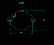
hi , heres the dwg file for plotters, yellow is origin, white pad (of course) ; )
Thx!
BK
Need insulation mat, as well as screws, THF-51S 2SK182ES bushing inside the ear, I can send it for free, (I can send a small number of accessories) can get free insulation pad, bushing, 4M screw.
Postage problem is the need for friends to pay their own postage
Postage problem is the need for friends to pay their own postage
to clarify ( a little) - pras is having gray silicone pads , M4 plastic isolator bushings and set of screws for your SITs , and all you need is to pay for shipping

now ZM : due to time needed for shipping ( me , receiving pads and bushings) , this turn I can't include the same with kits , but in future I'll have pads and bushings included .....
now ZM : due to time needed for shipping ( me , receiving pads and bushings) , this turn I can't include the same with kits , but in future I'll have pads and bushings included .....
Very generous of pras and ZM as usual!
As another option, here's a nylon shoulder washer at digikey that'll work with #6 and M3.5 screws:
MNI-6-6 Essentra Components | Hardware, Fasteners, Accessories | DigiKey
Note that the Tokin tab thickness is only 3mm, so any any shoulder washer longer than that will need to be either shimmed or modified to provide good clamping.
BK
length is not critical - easily done with any sharp (exacto?) knife/blade
though - that thingie is not practical for EU side of things , where metric is usual and non-metric tricky to obtain
in short - I prefer M4 for SIT , also prefer SIT bottom sanding on wet sanding paper on glass plate ... if using mica , of course
for silicon pad , no need for SIT bottom plate sanding
Last edited:
Cap return path
Hi ZM, was looking at your nice CRC supply boards and was wondering about the deep split in the ground, making the return of the high current pulses towards the first cap longer and pushes these currents close to the second cap ground connection and star ground point of the pcb... I'm sure you have a good explanation and am very interested in knowing why you did this.
Thank you!
.....
Hi ZM, was looking at your nice CRC supply boards and was wondering about the deep split in the ground, making the return of the high current pulses towards the first cap longer and pushes these currents close to the second cap ground connection and star ground point of the pcb... I'm sure you have a good explanation and am very interested in knowing why you did this.
Thank you!
point being that all pulsating current paths are more or less in form of bus between last two caps (with legs extended to first two caps) , while "tone" side of GND is moved from pulsating bus , more right
didn't had problems with that approach earlier , so why not repeating it ....
didn't had problems with that approach earlier , so why not repeating it ....
I offer here two pairs THF-51 that I do not need any more.
https://www.diyaudio.com/forums/swap-meet/328735-tokin-sits-2-pairs-thf-51s-sale.html#post5574057
Suitable for the SissySIT.
Thanks Zen Mod!
https://www.diyaudio.com/forums/swap-meet/328735-tokin-sits-2-pairs-thf-51s-sale.html#post5574057
Suitable for the SissySIT.
Thanks Zen Mod!
Latest info about packing and shipping
Babelfish M25 , AKA M2 on steroids , AKA M2-XA25 bstrd - kit packages
Babelfish M25 , AKA M2 on steroids , AKA M2-XA25 bstrd - kit packages
- Home
- Amplifiers
- Pass Labs
- SissySIT