KaBoom.........
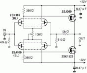
DO NOT RUN K389 AND J109 AT 32 VOLTS.
There also needs to be gate resitors on the mosfets and preferably the jfets as well I would cascode or series zener drop the drain voltages for the JFETs. I wonder if an amp from this schematic was actually built......
DO NOT RUN K389 AND J109 AT 32 VOLTS.
There also needs to be gate resitors on the mosfets and preferably the jfets as well I would cascode or series zener drop the drain voltages for the JFETs. I wonder if an amp from this schematic was actually built......
Picky... picky
The point was to make the gain asymmetrical to compensate for the the N channel mosfet having a greater transconductance. I believe you would want indentical open loop gains for each half of the circuit for lowest 2nd harmonic distortion. I believe the transconductance of the J109 is also a little greater than the K389 at the same current if I remember correctly. I don't remeber seeing this done before but I am sure it has been, perhaps even by Mr. Curl. The bias resisitors value will depend on the Idss of the Jfets and the value of the drain load resistors. I believe I stated that the would probably not be 75 ohms. I would try for at least 2 or 3 mA of bias current for each jfet and pick ones with Idss several mA above the bias current that they will be used at.
john curl said:Fred's biasing has problems. Not in concept, but in execution. The resistor values are too large, and the differential gain is asymmetrical
The point was to make the gain asymmetrical to compensate for the the N channel mosfet having a greater transconductance. I believe you would want indentical open loop gains for each half of the circuit for lowest 2nd harmonic distortion. I believe the transconductance of the J109 is also a little greater than the K389 at the same current if I remember correctly. I don't remeber seeing this done before but I am sure it has been, perhaps even by Mr. Curl. The bias resisitors value will depend on the Idss of the Jfets and the value of the drain load resistors. I believe I stated that the would probably not be 75 ohms. I would try for at least 2 or 3 mA of bias current for each jfet and pick ones with Idss several mA above the bias current that they will be used at.
Wrong Data Sheet......
The J109s are good for 30 Volts....... There are reasons for a cascode circuit besides just the drain to source voltage being too high.
The J109s are good for 30 Volts....... There are reasons for a cascode circuit besides just the drain to source voltage being too high.
FEts at high voltage
Hi hitsware,
JFets get noisy at high supply voltage because of leakeage, though not destructed. See the datasheet of f.a 2N5912 at www.vishay.com and Horowitz.
I learned it the hard way. Some form of cascoding will prevent this from happening.
😎
hitsware said:
Hi hitsware,
JFets get noisy at high supply voltage because of leakeage, though not destructed. See the datasheet of f.a 2N5912 at www.vishay.com and Horowitz.
I learned it the hard way. Some form of cascoding will prevent this from happening.
😎
http://www.ne.jp/asahi/evo/amp/device/2sj109.pdf
Oops.......See what you mean.......Strange they call them complementary? I like super simple so don't do cascodes.
.........mike
Oops.......See what you mean.......Strange they call them complementary? I like super simple so don't do cascodes.
.........mike
One reason......
Give that man a gold star. I was also considering power dissipation which is about 200 mW for these devices.
Give that man a gold star. I was also considering power dissipation which is about 200 mW for these devices.
The circuit should work, just as it is. Gate resistors are most probably optional on this design. Why? I don't know why you like gate resistors of jfets. All it does, in this case, is to make the input more noisy.
Simple is good, but not the best. This amp (post 81) will have pretty high distortion, driving gate-source capacitance of the Mosfets.
PMA said:Simple is good, but not the best. This amp (post 81) will have pretty high distortion, driving gate-source capacitance of the Mosfets.
I've done something simular (single ended 2sk170 driving Hitachis with no feedback) and got ~0.6% THD 20 to 20k. Not as bad as one would expect. (or get with IR types) IMO .... mike
Every type of device has it's own sweet spot(s). Don't
substitute devices into the same circuits and imagine that
you have a real comparison.
substitute devices into the same circuits and imagine that
you have a real comparison.
Nelson Pass said:Every type of device has it's own sweet spot(s). Don't
substitute devices into the same circuits and imagine that
you have a real comparison.
Ya Mon .... Forgot to mention used the Hitachis as followers ...
john curl said:The circuit should work, just as it is. Gate resistors are most probably optional on this design. Why? I don't know why you like gate resistors of jfets. All it does, in this case, is to make the input more noisy.
If'n you use a gate resistor with a jfet (at the input) ..... You get a rolloff that completely negates any kind of TIM .... I use 10K with 2sk170 .......
hitsware said:If'n you use a gate resistor with a jfet (at the input) ..... You get a rolloff that completely negates any kind of TIM .... I use 10K with 2sk170 .......
Hmmmm. But since FET input capacitance is so non-linear, wouldn't such a high value input resistor just acerbate the problem and produce greater amounts of high frequency distortion which could fold back down into the audio band?
A shunt RC network would ultimately be preferable, yes? Assuming of course that one's goal is optimal objective performance.
se
>But since FET input capacitance is so non-linear, wouldn't such a high value input resistor just acerbate the problem and produce greater amounts of high frequency distortion which could fold back down into the audio band?
It seems that would be the case, but in practice it works. It's a differant ball game than with something like the mundo IR type fets where the output (drain) reflects back to the gate. Using a 10kHz squarewave as referance, I get nice smooth response.
>A shunt RC network would ultimately be preferable, yes? Assuming of course that one's goal is optimal objective performance.
Yes, theorieticly. But sometimes to me super simple elegance in the schematic can outweigh other factors. I must say however I've not aurally A-B 'd the 2 approaches. Usually my squarewave approach is pretty dependable though...........mike
A question is if we consider THD of 0.6% to be low or high. For me that is high. How is the THD at 10 - 20kHz? Did you measure IMD - probably more problems with Mosfet's non-linear input capacitance.
PMA said:A question is if we consider THD of 0.6% to be low or high. For me that is high. How is the THD at 10 - 20kHz? Did you measure IMD - probably more problems with Mosfet's non-linear input capacitance.
For a 0 feedback (global anyways) amp, I consider it slightly high but workable. No I didn't measure IMD (or THD below 20Hz), so that could be bad, but again I've always had good results using carefull scrutiny of squarewave response.
hitsware said:
For a 0 feedback (global anyways) amp
what scematic are you talking about?
- Status
- Not open for further replies.
- Home
- Amplifiers
- Solid State
- Single or dual differential?