Lowest value I have right now I could try is 0R12, I will try it in couple days, i guess the bias current should be stable. 0R1 would be ideal, just a little bit of headroom.
Prasi, great this version looks much better.
There are 2 controls I`m gonna put on my version that could be useful and you could place 2 pin connectors on a pcb as a option.
First is to adjust the bias current with 3-4 position, rotary switch and second is toggle switch for bypassing degeneration resistor and changing damping factor. See the attached schematic for example.
Cheers.
Hello Bogdan,
For bias, I have added the option of either a dip switch or pads for pot to be wired to front panel.
Also made a provision for thick jumper wire for bypassing degeneration resistor.
For the cap bank, One can have either single big cap with film bypass or take it out and fit a cap bank.
regards
prasi
Attachments


Member
Joined 2009
Paid Member
Prasi thanks, looks great. (2SK932 is a nch jfet, not mosfet).
Bigun, yes the bass is tighter with degeneration resistor bypassed, (that's why I want to place that control switch on a front panel), tomorrow I'll do the set of measurements with degeneration resistor, to compare.
Beycoast ask Prasi about pcb files, it's fine with me.
Bigun, yes the bass is tighter with degeneration resistor bypassed, (that's why I want to place that control switch on a front panel), tomorrow I'll do the set of measurements with degeneration resistor, to compare.
Beycoast ask Prasi about pcb files, it's fine with me.
Yes, i didnt have proper device in my cad lib.
So here are all files if anyone wants to try.
So here are all files if anyone wants to try.
Attachments
-
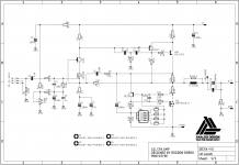
 SECFA-SCH-v3.png14.5 KB · Views: 230
 -
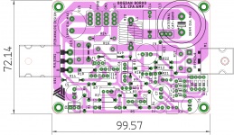 SECFA-LAY-v3.png84 KB · Views: 404
 -
 cap bank.png45.1 KB · Views: 398
 -
SE CFA-SILK-MIRRORED.pdf457.7 KB · Views: 131
-
SE CFA-CU-BTM-MIRRORED.pdf426.7 KB · Views: 123
-
SECFA-V3_2020-07-04.zip408.1 KB · Views: 105
-
CAP BANK-SILK AND CU-BTM-MIRRORED.pdf420.9 KB · Views: 127
-
CAP BANK_2020-07-04.zip84 KB · Views: 89
Prasi, sorry, I didn't said that feedback resistor, R11 is in fact two 0W6 metal film 390R resistors in parallel. It could be a single resistor also but with bigger footprint - 2W.
Hi Prasi,
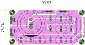
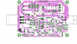
If I maybe a bit "up-myself" and suggest some slight changes to the ground tracking on the board, hmm?
There is the input signal ground points ("IN", R1, VR6,C3, C4), the input stage caps (C6 and C7) and the rail filter (C5), the separate R14, and the output group (C15, R24 and PGND) - these last bunch are okay and if you turn R14 vertical, you could "hitch" this one into the central/PGND area without too much change.
For another lot of work, perhaps you could relocate that ("IN", R1, VR6, C3/C4 group)towards the pair C6, C7, and maybe include that C5 in there too, and then link the lot of them to the central ground point with a separate copper link.
I don't know if this would make any difference to the overall sound/performance but I thought I'd mention it ....
, are 3 main Perhaps cut the trace between the "IN" socket ground trace and C5 and separately connect the whole input stage ground connections to central ground terminal via a direct wire link and maybe even C6, C7.
Maybe turn R14 vertical and see if it can be directly linked to split the ground track between C5 and R14 to central ground too
- ground track donut somewhere around C6 perhapsadd a donut between the "IN" socket and C5 to enable cuuting the trace tere and then
Hi Prasi,
If I maybe a bit "up-myself" and suggest some slight changes to the ground tracking on the board, hmm?
There is the input signal ground points ("IN", R1, VR6,C3, C4), the input stage caps (C6 and C7) and the rail filter (C5), the separate R14, and the output group (C15, R24 and PGND) - these last bunch are okay and if you turn R14 vertical, you could "hitch" this one into the central/PGND area without too much change.
For another lot of work, perhaps you could relocate that ("IN", R1, VR6, C3/C4 group)towards the pair C6, C7, and maybe include that C5 in there too, and then link the lot of them to the central ground point with a separate copper link.
I don't know if this would make any difference to the overall sound/performance but I thought I'd mention it ....
, are 3 main Perhaps cut the trace between the "IN" socket ground trace and C5 and separately connect the whole input stage ground connections to central ground terminal via a direct wire link and maybe even C6, C7.
Maybe turn R14 vertical and see if it can be directly linked to split the ground track between C5 and R14 to central ground too
- ground track donut somewhere around C6 perhapsadd a donut between the "IN" socket and C5 to enable cuuting the trace tere and then
Hello James,
Is this how you meant it?
I have also added 2 resistor option for FB or single larger one.
regards
prasi
Attachments
Yeah, that'll do it for R14 okay.
You could just add donuts for mounting the extra R11's one on top of the other, or one underneath the board too, if someone wants to play around a bit
The ground tacks for the "IN" and so on could possibly be grouped together a bit more but probably not worth the trouble
What's the 'spade connector under the C13 cap for?
You could reduce the RB switches to just 3 steps to give the 6 options (1, 2, 3, 1//2, 1//3, 2//3) or even just 2 switches for 3 options - just saying …
Nice neat work, as usual.
Yeah, that'll do it for R14 okay.
You could just add donuts for mounting the extra R11's one on top of the other, or one underneath the board too, if someone wants to play around a bit
The ground tacks for the "IN" and so on could possibly be grouped together a bit more but probably not worth the trouble
What's the 'spade connector under the C13 cap for?
You could reduce the RB switches to just 3 steps to give the 6 options (1, 2, 3, 1//2, 1//3, 2//3) or even just 2 switches for 3 options - just saying …
Nice neat work, as usual.
Undeath the C13 is option for connetor to the output cap bank pcb.
I think that 3-4 positions for the bias switch is more than enough, btw, it could be just 2 pin header on a pcb and with bias resistors directly soldered on the rotary sw.
Thanks.
The spade connector under C13 is an option to use external cap bank as attached in post # 48. In that case , C13/C14/R24 and 'OUT' spade are not mounted. They are taken care by the cap bank.
regarding dip switch, i think 4 position is most common in one's parts bin, it also allows using 2 or 3 position switch😉.
Very nice.
0.18Ohm is hard to get in thick film. 0.1? 0.22?
I installed 0R1 resistors, bias stability is very good.
Soon, schematic with edited, final values of components, and new measurements..
Thank you Vunce.
Last edited:
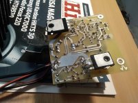
On the bottom layer of my proto pcb, under the one electrolytic, you could see layout for 1206 10uF cap for bypass, is this a bad idea or not? These caps are cheap..
Attachments
Last edited:
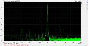
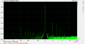
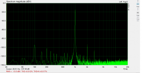
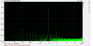
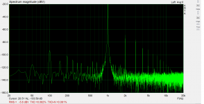
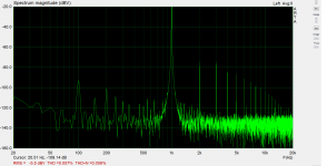
New 3R9 load measurements at 1A5 bias and +36V power supply.
Every level recorded with and without degeneration resistor DR- degeneration res. / NDR - no degeneration resistor..
Every level recorded with and without degeneration resistor DR- degeneration res. / NDR - no degeneration resistor..
Attachments
-
 1Vpp 3R9 DR.png62.2 KB · Views: 328
 -
 16Vpp 3R9 NDR.png36.7 KB · Views: 110
 -
 16Vpp 3R9 DR.png36.7 KB · Views: 99
 -
 8Vpp 3R9 NDR.png34.4 KB · Views: 88
 -
 8Vpp 3R9 DR.png34 KB · Views: 94
 -
 4Vpp 3R9 NDR.png34.1 KB · Views: 91
 -
 4Vpp 3R9 DR.png34.1 KB · Views: 99
 -
 2Vpp 3R9 NDR.png34.2 KB · Views: 95
 -
 2Vpp 3R9 DR.png34.2 KB · Views: 303
 -
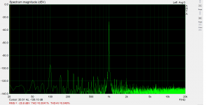 1Vpp 3R9 NDR.png34.1 KB · Views: 306
Last edited:
- Home
- Amplifiers
- Solid State
- Single Ended CFA