Storage time of a BJT is a well know effect that occurs when Ic<<beta*Ib. The excess base current causes a large charge to be stored on the base emitter junction (capacitance). A Baker clamp will keep Ic=beta*Ib and prevent the excess stored charge.
In a MOSFET Cgd becomes large at low d-s voltages or when the gate voltage is higher than the drain voltage. Again this is a well know effect and a result of basic physics.
So kenpeter, what are you talking about?
In a MOSFET Cgd becomes large at low d-s voltages or when the gate voltage is higher than the drain voltage. Again this is a well know effect and a result of basic physics.
So kenpeter, what are you talking about?
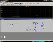
D'oh, how could this be complete without the Baker clamp?
Baker Clamp
Maybe even better with the recent zero recovery time SiC diodes (from Cree)... (I wonder if those would be good in the Allison too?)
I would never operate a power BJT at low Vce, because simulation and datasheets readily show the bad behavior. However I understand saturation only becomes a problem at say >40mA as long as you keep above Vcb=0. It sounds to me like saturation occurs when the BC junction begins to forward-bias, and this causes the transistor to lose most of it's redeeming qualities.
Those are VDMOS models, not EKV, if I am not mistaken. LTSpice added some parameters to include subthreshold simulation some time back, I remember on the yahoo group...
Diffusion delay sounds like series resistance, sort of... Thermal transfer in power semiconductors is a diffusion process.
Looking at the switching times from this datasheet doesn't seem to indicate low Vce=low switching speed, given appropriate base drive. The problem is finding datasheets with detailed switching charts, for transistors not unlike those we use in audio.
http://www.fairchildsemi.com/ds/2N/2N3904.pdf
- keantoken
SIC Schottky forward voltage is over 1.5V, no dice that way.
Great at high temps, insane voltages, and no recovery glitch,
but definitely not a low drop. Probably the bandgap...
Look , I don't really know if Ts is relevant here or not. The
thing causing me confusion is two incompatible definitions of
BJT "saturation". One says when VCE<=VBE, the other says
when an increase in Ib no longer increases Ic. Not the same,
yet you will readily find both definitions if you search. I now
suspect Ts only relevant at the latter defintion.
We still have to ask what happens at the collector junction
as it becomes partially forward biased beyond the first def?
Surely this must at least change the Miller capacitance as a
varactor? I'm betting dimensions of base are changing at that
interface as well.
Why would we operate a device we wish to be linear on the
threshold of so many parameter changes? It is no big deal to
add one diode or transistor drop of extra voltage here and be
completely free of the question.
And if it weren't already clear as mud, what happens when
there is added layer of epitaxy between base and collector?
Does this eliminate the depletion region at the collector and
render meaningless the VCE<=VBE definition of saturation?
I don't fully understand what magic an epitaxial layer might
or might not do.
-----
Back cover of Cordell's book says EKV models. Are they same
or different than the VDMOS ones on his webpage? I won't
have that book in my hands any sooner than Monday lunch.
Last edited:
I think saturation is the latter definition, with the first definition not being accurate.
If you look at datasheets, you will readily find the VceSat graph. This will tell you the Vce where Beta falls to 10. I see this as hard saturation, where the transistor begins to stop behaving like a transistor. Another is the Vce-Ic graph, where you can see the Beta of the transistor is roughly dependent on Vce until about 2-4V.
Usually, VceSat is below 10mV for small-signal applications.
Here is a special graph. Bottom axis is Beta, Y axis is Vcb. Beta begins to die at about -300mV. Vcesat for this model was reasonably close to this datasheet, and I haven't had any indications that this is unrealistic.
- keantoken
Attachments
Then you can start by correcting Wikipedia.
Bipolar junction transistor - Wikipedia, the free encyclopedia
What about the Baker Clamp page you linked?
Hints at possible cause for VCE<VBE as "saturation" mixup?
http://home.mira.net/~gnb/audio/bakerclamp.html
"However, high voltage power transistors exhibit a quasi-saturation region
caused by stored charge in their wide, high resistivity collector region.
When operated in quasi-saturation, some storage time still occurs."
How were high voltage transistors constructed at that time? Did they
have a wide depletion region, or an epitaxial layer of undoped silicon?
He sais it was ripped from an OnSemi document dated 2001, but were
they in turn merely quoting Baker or other text from an earlier time?
Every silicon collector I've ever measured, acts just like a PN diode.
Whatever epitaxy is supossedly doing, it ain't a simple insulator.
Last edited:
The Baker Clamp provides the expected results for low-voltage bipolar transistors - that is, storage time becomes negligible and fall time is not affected. However, high voltage power transistors exhibit a quasi-saturation region caused by stored charge in their wide, high resistivity collector region. When operated in quasi-saturation, some storage time still occurs. It is possible to move operation out of the quasi-saturation region by stacking additional diodes in series with DB, but the on-state loss becomes unacceptably high.
Baker Clamp
It sounds here as if the time constant is caused essentially by the ESR of the junction capacitance. But the article says this only applies for high-voltage power transistors.
Saturation: With both junctions forward-biased, a BJT is in saturation mode and facilitates high current conduction from the emitter to the collector (or the other direction in the case of NPN, with negatively charged carriers flowing from emitter to collector). This mode corresponds to a logical "on", or a closed switch.
Bipolar junction transistor - Wikipedia, the free encyclopedia
These all describe saturation by it's symptoms. It seems clear to me that hard saturation is when the B-C junction of a transistor begins to act like a forward-biased diode, ruining the entire behavior of the transistor. When this happens, the recovery time and other time constants in the B-C diode contribute much more to the final operation of the transistor.
"Storage charge" is a fancy term but it doesn't tell us crap about what actually is happening in an electrical sense. It is just charge? Is there a series resistance with the charge? Is it a limit on the speed of electrons? Is it a dynamic impedance in series with the junction capacitance?
I think a dynamic impedance is most likely the case. In the match, it appears that most webpages forget about seeing time constants as impedances and just try to get on with mimicking the curves. As a result, what we see are confusing abstractions we can't relate to. I am sure someone could lay out the math spice model as a set of IV sources, capacitors, and resistors that that would make things very clear. Surely it's already been done, with the most modern models.
Perhaps it is possible to understand by visualizing the junction capacitance. A thicker dielectric (depletion region)=more resistance=larger time constant. Higher voltage transistors need a thicker dielectric, which seems to agree with the Baker Clamp article. But, this means small-signal transistors are fine, right?
Then you can start by correcting Wikipedia
I think sawreyrw should do it, he seems to know all this.
- keantoken
Also, as I understand it a diode is considered forward-biased if it has a positive voltage across it, even if this voltage is not enough to turn it on. This may be why they say saturation is when Vcb<0. Just a guess...
- keantoken
- keantoken
Keantoken,
Doubt this helps (its been a long time since I've thought about BJT saturation and I'm not sure where there is or if there is confusion) but...
I think that saturation occurs as the collector base junction goes from reversed biased to forward bias. One of the consequences is the emitter to base current (at least the electrons for an npn) no longer gets swept up to the collector and rather goes into the base-emiiter region (and can be thought of as stored charge), similarly another base to collector current now begins to flow. Both effects not only degrade apparent current gain but need to have all the carriers removed from the base region in order to return to the linear mode.
I thought most Ebers-Molls models exhibited this effect.
You can verify the model at least shows the related storage time effect (removing the excess base current), just drive a simple npn with into saturation with a source and series resistance then quickly change the source voltage while monitoring the base voltage. The base voltage should approximately hold constant until all the excess base is removed , and then exhibit a typical RC decay determined by the drive resistance and the b-e junction capacitance).
You can similarly measure the excess charge by putting a speed-up capacitor across the source resistance until the turn-off delay goes to zero then the delta-voltage x capacitor will be equal to the charge removed.
Actually with simulators I suspect there are a lot of more direct ways to measure the charge (i.e. drive it with a current source).
Indeed its been a while please don't take any of the above to literally.
p.s. Relatively new to the forum, so I've been doing lots of thread catch-up reading and have really enjoyed and learned from your postings.
Thanks
-Antonio
Storage time and stored charge in the base emitter junction can be explained by semiconductor physics, but that has never been a strong point of mine. When a transistor is saturated, an electrical model of the base emitter junction is that it is a source of charge. When you reverse the base current from a saturated transistor, Ic and the base emitter voltage will not start to change until the reverse base current removes the charge. The time to remove the charge is Qstored=Ibreverse*Ts; it's really the integral of Ibreverse*Ts. LTspice will show you this effect.
Anyway, you don't want a transistor saturating in an audio amplifier.
Anyway, you don't want a transistor saturating in an audio amplifier.
In critical places transistors should have at least 2-4V across them to get out of the Early-slump region.
To my knowledge the transistors in that CCS are not saturated, even though Vce is 0. If this was not modeled correctly I'm sure I would have heard about it by now.
What I don't get is why everyone uses the terms "storage charge", when "capacitance" would be just as good, and "storage time" when "time constant" would be just as good. All this unnecessary jargon just keeps us in the dark. It seems to me that the problem is a capacitance which gets filled up during normal behavior, but then is difficult to discharge when saturation occurs and causes a dynamic series resistance with the capacitance. Or is it that the series resistance doesn't change and the capacitor becomes several times larger during saturation? I really don't see any way it could be except a dynamic capacitance and resistance, and an explanation in these terms would probably be to the edification of DIYers everywhere. And I know Kirchoff's Law still applies, so there can't be any goofy physics of getting out any more or less holes or electrons than you put in, right? So let's just return to familiar electrical theory without any unnecessary complications. Is it effectively a dynamic RC time constant, or not? My intuition is that this can be a great deal simpler than it is presented, at least to the DIY crowd.
A diode with 1mV forward bias, will be forward biased, yes... But will it actually be turned on? Probably not measurably. 100mV? Maybe for germanium types. At 200-300mV is where it may actually become important, depending on your application, and this is if you are requiring great precision. This is also indicated by the simulation models, where real saturation begins to occur at no less than -300mV Vcb.
For power BJTs, running low Vce is undoubtedly bad. For small-signal ones I don't think so.
- keantoken
Last edited:
Keantoken
Sorry didn't mean to add jargon. From my view I guess it's closest to a dynamic capacitor on top of the normal Vbe which gets filled by the base current when in saturation.
Low collector voltages decrease beta and that portion of the base current goes into charging this capacitor rather than getting multiplied up to the collector.
Hope this helps
-Antonio
To my knowledge the transistors in that CCS are not saturated, even though Vce is 0. I
Again I'm relatively new to the forum as well as many of the acronyms, but if CCS refers to a constant current source with one BJT having its collector tied to the base Vcb = 0 then the Vce still has some potential relative to the emitter and the beta action of the transistor will prevent saturation.
Hope this helps
-Antonio
In the case of Allison: As long as the output device presents two emitter drops of
threshold to turn on (Darlington pair or enhancement MOSFET), error amp collector
stands plenty high enough. With bootstrap, no excuse VCE<VBE ever need happen.
Still would affect output device as it approaches the rail, no bootstrap help here...
But thats same for just about every amp...
Strange you would obsess on .0000000000000000000000013% distortion, and yet
be OK with operating a small signal transistor in a region where its been cursed by
the evil eye. Damn the real world physics of it!
Last edited:
Magnoman, welcome to the forums. Here is the CCS I'm talking about:
http://www.diyaudio.com/forums/soli...lison-based-output-stages-12.html#post2492348
If we see the transistor as 2 diodes, then Vce=0 should roughly be where all transistor action stops. I've found that the breakover voltage of the B-C and B-E junctions aren't always the same, so this relationship is not precise.
The text you quoted contains an error I made, I meant to say Vbc. I keep mixing them up!
Your explanations are helping. You seem to be confirming my suspicion that when the B-C diode becomes forward biased, it's recovery time and time constants (not to forget natural diode action) are what degrades the net gain of the transistor, even though the B-E junction is behaving like any normal diode. But this would mean that charge is stored in the B-C junction, not the B-E junction.
So far none of this points to driving small-signal transistors at Vcb=0 as a bad idea, all other things considered.
You say that it's closest to a dynamic capacitor on top of the Vbe junction. Do you mean in series with the base? Parallel to the B-E? Parallel to the B-C?
If I seem angry or annoyed, I am not and didn't mean to come off that way. We are making progress.
- keantoken
Kenpeter, I have found that the beta of the Allison transistors is unimportant, as long as they have normal transconductance (the bases are connected to a very low-impedance high-drive node). This is true if you don't use a very large resistor in series with the base for compensation.
Most of us know that transistors are more linear with more than 2V Vce. However I never heard of an abrupt decrease in speed below this. Where do you draw your conclusions from, and where can I read about this?
- keantoken
Most of us know that transistors are more linear with more than 2V Vce. However I never heard of an abrupt decrease in speed below this. Where do you draw your conclusions from, and where can I read about this?
- keantoken
My father is dead (Harley D. Peter - Engineering Fellow Raytheon/E-Systems).
Helped design a surveillance receiver abused by Nixon to spy on Watergate.
http://watkins-johnson.terryo.org/CEI-Receivers/RS-111.htm
Designed and wire wrapped his own 20MHz minicomputer in 1973, compatible
with DEC PDP-8 instruction set. Nobody had a 20MHz computer then, NOBODY.
I should say he finished it in 73, obviously that didn't all happen overnight.
I can't ask him specific details why he taught me that rule. All his technical
books and handwritten notes are wherever his wife decided to dump them.
Mint Radiotron Designer's Handbook 4th ed, gone who knows where...
Hundreds much rarer texts, optics originally worth tens of thousands scratched
and broken. Sometimes I get a call when something she thinks is important hits
the curb, most of the time not. Its all just garbage to her, and our relationship
is one of smoldering hostility.
He said don't do it. Therefore I don't need a logical reason for my conclusions.
Last edited:
keantoken,
I can't describe BJT storage time effects much better than I did in post 608. What don't you understand about it?
Rick
I can't describe BJT storage time effects much better than I did in post 608. What don't you understand about it?
Rick
All I know is that it is taking time for electrons to get from here to there. I want to characterize this phenomenon in terms of a dynamic reactive network. This would be meaningful for me and others in the hobby, and help me to know what I need to do to adjust to it.
- keantoken
- keantoken
Member
Joined 2009
Paid Member
There are a few threads around which talk about the Allison - but no conclusion for the mortal man - no 'final circuit' or 'stay away from this' warning - where does it all end ?
The Allison doesn't seem very popular ?
The Allison doesn't seem very popular ?
No one has stepped forward to build the circuits and test them. I suspect many of them will be difficult to stabilize without sacrificing linearity.
Ultimately the Allison itself is just a buffer. Buffers are of limited usefulness, and it's not really surprising for buffers to have extremely low distortion. Add to this that the stability issues can become very complex with high-current versions, and you have a project that can go to absurd levels of tediousness. Also consider that the Allison inherently will have a high output impedance.
That said, it can be simple enough to be well worth a try if it's for a signal buffer like my Kuartlotron in my signature.
The question is, where is it most useful? IE, where would most people use one if they had it?
Kean, this is Allison on the driver in the proven Adcom GFA-555 original, page 5 of the .pdf:
http://akdatabase.org/AKview/albums/userpics/10007/Adcom GFA-555 Service Manual.pdf
This amp has proven to be very reliable, I own 2 of them and it was one of the most
popular entry high end amps.
http://akdatabase.org/AKview/albums/userpics/10007/Adcom GFA-555 Service Manual.pdf
This amp has proven to be very reliable, I own 2 of them and it was one of the most
popular entry high end amps.
- Home
- Amplifiers
- Solid State
- Simulation Analysis of several unique Allison-based output stages.