Fantastic results.
Did you use NOS BG or did you save them from previous experiments ?
If these are NOS, how long did you burn them in ?
Did you use NOS BG or did you save them from previous experiments ?
If these are NOS, how long did you burn them in ?
No aren't NOS, are from older projects so are burned.
Imagine the BIG change BG does that now I have to adjust the value for C2 RIAA capacitors: after 16nF024 now 15nF977 & possible will finish 15nF930 or less.
Imagine the BIG change BG does that now I have to adjust the value for C2 RIAA capacitors: after 16nF024 now 15nF977 & possible will finish 15nF930 or less.
Just finished my main PCB according Salas instructions.🙂
I attached files for main, copper and silkscreen in PDF format.
Right now I gonna prepare my self to etch my first PCB.
Nice work !
Please post some pictures of the pcb (after you etch them).
Nice work !
Please post some pictures of the pcb (after you etch them).
Yes, it looks good.
But a comment to the grounding: afaik it is not good to change from wide traces to narrow traces and vice versa.
Specially not when currents are flowing, what is the case for the grounding, specially between the bypass caps.
Franz
/Edit: try to explain (afaik): different size of traces is resulting in minimal differences of conducitvity eg. resistance. When currents are flowing this will produce voltage differences on the grounding traces. And this is to be avoided. Better use one trace width, as large as possible.
Last edited:
BOS might be even better than NOS 🙂
Everything depends on the burning.
The burning was doing with 1st quality wood (ebony) & slow fire to cook the cap as better as possible.😀
@NPower
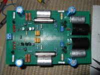
In your pcb I don't like IN gnd + RL gnd not referred with thier own track to star gnd. If you connect them to D4 gnd and R2V gnd, you mix up Signal gnd and Power gnd. Not good at all.
Take example from OUT gnd and R8 gnd: correct routing.
Plenty of space to fix this problem....
In your pcb I don't like IN gnd + RL gnd not referred with thier own track to star gnd. If you connect them to D4 gnd and R2V gnd, you mix up Signal gnd and Power gnd. Not good at all.
Take example from OUT gnd and R8 gnd: correct routing.
Plenty of space to fix this problem....
You did not forget the garlic did you ? 🙂
I forgot thanks for advice I will do "a la llauna" catalan typical foot🙂
Cod (bacalao), not snails, I hope! 😉
Nice typo: catalan typical foot 😀
Some of those are now on TV.... vs Switzerland!
Nice typo: catalan typical foot 😀
Some of those are now on TV.... vs Switzerland!

Cod (bacalao), not snails, I hope! 😉
Nice typo: catalan typical foot 😀
Some of those are now on TV.... vs Switzerland!
Cod of course.🙂
Smile...
Indeed, I am not interested in football. But I was in a local bar, drinking beer.
And this was fun, a big surprize.
Franz
BTW:
My audio chain is sounding awesome, actually...
Indeed, I am not interested in football. But I was in a local bar, drinking beer.
And this was fun, a big surprize.
Franz
BTW:
My audio chain is sounding awesome, actually...
I am listening to the Wall, Pink Floyd, dear Salas! With great pleasure with the simplistic amp, optimized tonearm mass (thanks to my spanish friends), best available analogue crossover, big speakers.
Nice sovjet caps on your board 😉
Bypass or also for RIAA?
Franz
Nice sovjet caps on your board 😉
Bypass or also for RIAA?
Franz
- Home
- Source & Line
- Analogue Source
- Simplistic NJFET RIAA