Better no capacitance if not mandatory.
If it has to be there, interface it with 10-100R in series to become an RC not to interact with the reg's HF termination so not to slow it down.
Thanks,
OK, I will route these three capacitors (30 uF 500 V MKP) to the input of the CCS then.
Then: Each earth line of each stage goes separately to the star ground and each tube anode resistor is connected separately to the SSHVshunt.
No extra caps (not even a mica 😱 ) on the amp board.
albert 🙂
Route them closely physically across the input of the CCS. Small caps without extra loss introduced on the rail are going to "short" the Zobel termination on the reg if there is not much real parasitic inductance in between to really decouple. Usually the best results come when there are no not really needed components after the reg.
Hey Salas,
Hope you're well. I have a slight issue with my SSHV2 incarnation. I'm using the SSHV2 to provide a stable reference for my 4-65a SE amp which is DC coupled. The regulator needs to provide 260-280V @ 70mA. It is driving two 46 in filament bias with gyrator loads. Each one running at 30-35mA. The SSHV2 is stacked with a second power supply (180V) to provide grid current for the amp.
The SSHV2 was modified slightly as described here: 4-65a SE Amp: Shunt regulator | Bartola Valves
I'm using a IXTP01N100D for top FET and also STE5NK100Z for the pass FET. I can only make the shunt voltage to 260-270V. Not 280V as originally planned. The CCS current is at maximum and gets to 100mA. I have a ammeter at the input of the SSHV board. I think one of the issues I have is that the pass FET has a tiny L-angle aluminium piece as a heatsink. I should use a proper heatsink I believe. The regulator starts at 95-100mA and then after running it for some time it drops down to 80mA. Surely this is due to pass FET getting really hot, correct? Then I get some random spikes on the output stage currents and I can see that the SSHV2 loose it regulation and voltage drops and pops up some 10V and then go back to normal.
Will this just be the drift effect of poor heat dissipation on the pass FET?
Thanks
Ale
I am well, hot summer here. Thanks.
There are semiconductor type changes in your incarnation that I can not speak of from experience but only speculate about their integration of course.
Dropping some CCS mA with warm up must be due to Vgs VS Tc changes in the CCS cascode, not in the "pass" shunt element. Maybe you drop much unnecessary Vin-Vout?
That would create excess dissipation when just 20V across is fine. You can also change the 10R T.P. resistor to 1R for extracting a bit more top CCS. You should translate mV for mA X1 not X10 for T.P. CCS readings after that of course.
I also see that your FP plastic back package ST shunt MOSFET choice has different parasitic capacitance plus embeded gate Zeners. But I wouldn't be suspicious about the SuperMESH MOSFET first. Use a tiny drop of CPU grade thermal grease at its back if you haven't already nonetheless. What is its max case temperature?
The reluctance to go 280V would be either you have chanced upon a really low Idss JFET (see to have a ~4mA testing sample) or your load hovers very near to to your max CCS even before the warm up loss and you experience a ceiling for Vo setting plus periodic drop outs at peak demand occasions.
Have you got data about the actual load demand?
I will try first a proper heatsink for the FET and also measure temperature. I think now is about 70C.
You're probably on the right path regarding the CCS power dissipation. I think I'm dropping more than 20V (need to check input voltage) but running at nearly 90mA is getting really hot. This will make the CCS drift then.
Regarding the load, it's a IXTP01N100D single FET gyrator connected in mu follower output. The mu-follower resistor is 820r which is then connected to the 46 valve. I measure about 29V across the 820R which is 35mA per valve.
I will do proper measures on voltages and come back to you on this!
thanks for the help
Ale
Can only make it stable running at Vout=246V. Vin is 347V. Input current is 90mA. Temperature of CCS heatsink is 72C and shunt FET heatsink is 50C. CCS is dissipating about 7W. Shall I look at reducing 50V the input voltage then?
Thanks
Ale
Thanks
Ale
Yes. Lose some on an RC cell. It will do good to incoming raw DC ripple level and harmonics too.
Changed secondary winding and achieved 274V raw at full load. Not ideal, but high enough without modifying the raw supply filtering to get some volts back. After some adjustments to bias settings and allowing the system to warm up properly I got stable voltage regulation at 244V output (30V drop across the CCS) and the CCS current drop from 90mA slowly to 80mA and heating up from 45C to 56C. The shunt fet temperature is about 44C which is fine. Clearly the IXTP01N100D is playing here as probably the heatsink is not that big to work at 80-90mA high. I also run out of headroom to increase current on the CCS when the FETs are hot, so I may need to change the sensing resistor as you suggested.
Thoughts?
Ale
Thoughts?
Ale
Just change the sensing resistor to 1 Ohm now. Looks like it will push the borderline just so that may prove a good help.
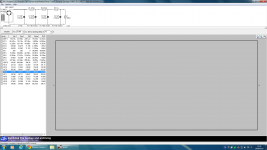
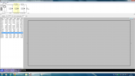
I want to know if a RC filter 1 ohm 3uF between SSHV2 & load can affect the perfomance of the reg.?
Fitting a filter after the regulator won't affect the performance of the regulator.
The load will see a different source and thus the load may perform differently.
The load will see a different source and thus the load may perform differently.
Fitting a filter after the regulator won't affect the performance of the regulator.
…
It may affect the supply to the client.
I know the load perform different that's the reason I want to use a RC filter but I'm not sure if the load can't see more ripple, could you elaborate?
Last edited:
In my PSUDII simulation the last RC 1 ohm 3uF just before the load increase the ripple.
Last edited:
Merlin, your simulation doesn't take into account the SSHV. The preceding RC strings in your simulation can't supply additional current in the min extremum of the pulses due to passive nature of filtering. SSHV is an active device, which can compensate the additional current from the shunting element. The only problem - the speed of the compensation. In case of additional RC string it's lower than with direct connection. As you can see in this case the problem is the circuit to be powered, not the power supply side.
That's the reason I want put the RC filter after the SSHV2, the only doubt that I have is if the RC filter adds or not adds ripple after the SSHV2 and why?
There is no need to lower the ripple over what SSHV2 does.
Adding an RC filter after SSHV2 will slow down it's own correction, thus, it will lower its' benefit.
Adding an RC filter after SSHV2 will slow down it's own correction, thus, it will lower its' benefit.
- Home
- Amplifiers
- Power Supplies
- Simplistic mosFET HV Shunt Regs

