mjona points to a way of rescuing this circuit. Without changing much to the existing stages, you can add a PNP input transistor to eliminate the non-linearity issues of a two-NPN input stage. There are some additional bias changes to be made to achieve this, but I suggest they are worth the trouble.
The changes needed, as I envisage it, are:
1. Provide a bias voltage for the PNP base using a 27k and 22k divider across the supply rails. This gives something a little below half Vcc, but the differences are taken up by the PNP emitter-base and feedback resistors.
2. Decouple the bias voltage to ground with a capacitor e.g. 100uF. This also provides a slow turn-on to avoid thump./
3. Add another 22k resistor between this bias junction and the base of the PNP.
4. Take the emitter of the PNP through two 1k resistors to the centre rail.
5. At the junction of these 1k resistors take a feedback "grounding" resistor depending on the gain you want. This would be 27 ohms for approximately teh same gain as before (~40) or 47 ohms for a gain of ~20. Use a 1mF decoupling capacitor in series to prevent DC feedback.
6. The collector of the PNP now goes to the base of what was T1.
7. The biggest changes are to the bias resistors on what was T1 and T2. The input impedance to these two base-emitter junctions is very high. Typically T2 will have an impedance of about 500ohms, but that pushes the input impedance to T1 up to about 50k. So any usual value of resistor like 2.2k is going to shunt the signal. Therefore, use a 47k resistor BUT this has to be taken to a negative supply line of about the same voltage as the supply, e.g. -50V. Even this resistor is lower than desirable, but far better than nothing.
This additional supply rail can easily be generated from the original power supply (if it is a standard transformer-bridge-capacitor type) by adding voltage doubling components (two diodes and capacitors), and possibly a supplementary RC filter, only referencing the "doubling" voltage to zero.
8. The base bias resistor of what was T2 should be changed to 1k.
9. The emitter resistor of what was T2 can be removed, along with the capacitor as the new feedback provides great DC stability.
10. As the negative rail could exceed the reverse breakdown of T1, in adverse conditions, an advisory diode (1n4148) should be wired in reverse across the base of T1 to ground.
11. The original feedback and bias resistors (two 100k's, 22k and 390k) are not required.
12. High frequency stabilisation can be accomplished by connecting a 47pF capacitor between the output rail and base of what was T1.
This is called "output inclusive Miller" compensation. Normally, Miller is not my preferred method of stabilisation, but in this case, the first 1k resistor in the emitter of the PNP provides massive degeneration and avoids transient distortion completely, and in my view makes it "safe". The compensation scheme is so effective that even with bootstrap resistors and quasi-complementary outputs, crossover distortion is almost completely absent (further improvements can be done, though) and overal THD with a gain of 40 is about 0.02%, and around 0.04% at 1V output- better than an order of magnitude improvement from the original. (Simulated results).
I think you will like the audible performance of these changes, as I once built a stereo amp some time ago with this concept, and that sounded "pretty good". As far as I recall, the 1kHz distortion was around 0.02% as measured, but I'd have to dig out the results to be sure.
I'll publish a diagram if interested.
Last edited:
good morning all, thanks for all the help. I have checked the voltage at the collector of T1 and with a supply of 50v it is sitting at 8.5v. But the be voltage of T1 is sitting at 0.35v, I would assume that the be voltage of T1 would be determined by the voltage divider made up of R15/16 and R3 would changing R15/16 to 47K help? . John I did scrape some cash together and purchased a Picoscope 2205A hopefully that will help with distortion adjustments . It would be great if you could post a diagram
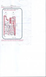
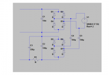
Voltage doubler.
I've only shown the basic circuit. V1 is really the transformer secondary.
The filter resistor should be 1k.
I could not help but suggest a full wave voltage doubler as it only needed one extra capacitor, and a second small low current bridge rectifier rather than individual diodes.
D1-D4 are the main power rectifiers. D5-D8 can be a 0.5A 200V or higher bridge.
Attachments
Last edited:
good morning all, thanks for all the help. I have checked the voltage at the collector of T1 and with a supply of 50v it is sitting at 8.5v. But the be voltage of T1 is sitting at 0.35v, I would assume that the be voltage of T1 would be determined by the voltage divider made up of R15/16 and R3 would changing R15/16 to 47K help? . John I did scrape some cash together and purchased a Picoscope 2205A hopefully that will help with distortion adjustments . It would be great if you could post a diagram
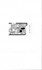
As far as I can tell the board image you posted is from the component side and although there have been some changes in the routing of the traces the only difference between this and the kit version is the omission of a couple of 1N4007 diodes in parallel with R14 and R13 - which in any case make no sense. TIP3055's should work as replacements for BD243C so your work looks all good to that point.
When I first looked at this circuit my initial thought about the lower NPN not turning on was R16 should be 4.7k and R5 should be 18k rather than the other way around. This will lift the collector voltage at T1 as more current will flow through 4.7k and less will be diverted around T1 with 18k to block that route through R5.
Trying this is a whole lot easier than modifying your circuit so you might consider this before going along that route.
To do this I suggest removing the fuse from the supply rail holder and either clip or solder a safety resistor of 100R of value 1W between the holder ends and see if you can get the dc side of the output close to 20 volts.
Last edited:
John thank you for all the assistance. Mjona I swapped the 4k7 and the 18k as suggested and this has resulted in a voltage of 39v across CE of T1 instead of 8.5v with a current of app 2.5mA. However T1 is still not on and I think this is the cause of all my problems. Would increasing the value of R4 help ? I have current limited psu so I did not install a safety resistor. Does any one have a copy of the original RCA circuit ? Thanks
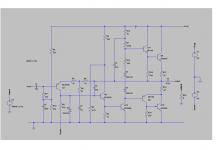
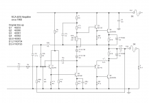
The circuit you have got is an almost exact copy of the RCA design. I have attached a copy of my reworked version which only updates the components. The diodes on the output 1 ohm resistors were to improve quiescent current stability, but help to cause distortion. The circuit was designed before RCA discovered the Vbe multiplier, and it is surprising that the original is still around without this update.
The 4.7k and 18k are shown correctly. As I pointed out in an earlier post, there is enough current (even with a 2.2k base resistor, the original was 4.7k). (The 40233 was only rated to 18V!)
The collector voltage of T1 should be around 8V which I think you measured before. That would suggest that T1 is working (the OC voltage with no current in T1 is 10V; you can check the currents by measuring the voltage across the 18k and 4.7k independently).
What meter are you using to measure the base of T1? It should be a digital meter with ideally 10Meg input. Many of the cheapies only have 1Meg, but that should be good enough across 20k. An old Avo (perhaps you don't have one, I still do) would not work on 3V range as it is only 60k.
If that does not show anything can I suggest you check the resistor values and whether the transistors are functional.
The best way to check the resistors is to lift one end from the PCB so that you aren't looking at anything else connected. I think the problem is around the bias and feedback. Sometimes reading the new 5 band resistor colour code can be confusing. Or 4 band if you've got used to reading 5 band.
Attachments
Hi John I did my apprenticeship on Avo8 about 33 years ago as radio technician. At the moment I have a GW INSTEK GOS 122 scopemeter and a Fluke 287 and a Picoscope 2025. Thanks for posting the circuit as I can see it's exactly the same, one thing I have noticed is having no load ( 8 ohm speaker ) does seem to affect the operation of the circuit. With R16 and R5 in there correct positions I was measuring app 8.5v across CE of T1 and 0.35v across BE of T1 although from calculations it should be closer to 1.2v does T1 cause a almost 0.85v drop ?
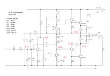
Circuit attached with simulated voltages annotated for 50V rail, assuming 0.47 ohm emitter resistors and no diodes.
Attachments
Last edited:
one thing I have noticed is having no load ( 8 ohm speaker ) does seem to affect the operation of the circuit.
Yes with a speaker connected approx. 6uA will flow through R6 (390K) and the speaker and alter the midpoint voltage slightly . R6 relates to the original schematic and not the above just posted version .
Last edited:
Another reason not to take feedback from the output capacitor!
I'm wondering if you have oscillation problems. The circuit was stable as far as I recall (which used 2N3055H's back then) but modern 3055's and the TIP3055's are faster. The circuit should be just as stable, however, but sometimes wiring layout can give unwanted effects. With your scope on the output measure the voltages again and see if oscillation occurs either before or after attaching the meter leads.
I'm wondering if you have oscillation problems. The circuit was stable as far as I recall (which used 2N3055H's back then) but modern 3055's and the TIP3055's are faster. The circuit should be just as stable, however, but sometimes wiring layout can give unwanted effects. With your scope on the output measure the voltages again and see if oscillation occurs either before or after attaching the meter leads.
I changed R3 back to 22k after finding that connecting the speaker does affect the midpoint which is now sitting at exactly 25v. There does not seem to be any oscillation until I put my meter leads on the base of T1 which then causes a loud buzzing from the speaker and the output stage starts heating up very quickly.
The base of T1 is the most sensitive part of the circuit, and is prone to pick up as the impedances around it are all high (10k, 22k, 100k...). So if the centre rail and quiescent current can be set properly, things should be working. Is that the case?
It looks like your meter leads cause oscillation which can cause the D.C. readings to be out.
It looks like your meter leads cause oscillation which can cause the D.C. readings to be out.
A possible way of checking the DC conditions without disrupting the signals might be to probe the input through a 1M resistor. You will need to adjust the reading to account for this: e.g. 1M multiply by 2, if 10M multiply only by 1.11. I'm not sure what your meter is (I haven't looked up its spec).
Or temporarily wire a capacitor across T1 base to ground, e.g. 10uF. It will need a settling time, and disconnect it after making the measurements.
This should not be necessary if the amp now works though.
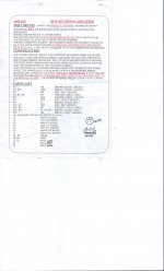
In my archives I have a document "RCA Power Transistors- Typical Audio Amplifier Circuits". It includes the 40W circuit and a 70W design of unmentionable quality. I came to view those as an RCA horror show.
Or temporarily wire a capacitor across T1 base to ground, e.g. 10uF. It will need a settling time, and disconnect it after making the measurements.
This should not be necessary if the amp now works though.
In my archives I have a document "RCA Power Transistors- Typical Audio Amplifier Circuits". It includes the 40W circuit and a 70W design of unmentionable quality. I came to view those as an RCA horror show.
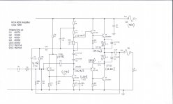
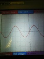
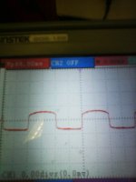
I have attached a copy of the original diagram with my voltages in brackets. I have attached pics of my scope images at the base of T6 and T5. At T6 the waveform appears as normal but at T5 the waveform is distorted and at a considerably lower level when the bias current is increased the waveform at T5 base gets smaller and eventually disappears at maximum bias setting
Attachments
- Status
- Not open for further replies.
- Home
- Amplifiers
- Solid State
- Simple circuit help