Excellent, Richard (retailer). There were some uncertainties about the winding directions in the Z565 layout, so it would be great if you can document your build in detail. Best regards
I've also seen some discussion on various forums regarding the winding direction of the primary and secondaries on Dynaco output transformers - opinion seems to vary - I'm not inclined to unwind one of the output transformers in my Dynaco SCA35 to check so I've gone by various bits of info found on forums.
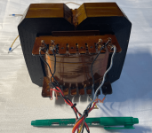
There was a discussion about the winding directions over on audiokarma, a forum member rewound a Z565 and documented the rewind project with windup diagram, turns count, wire size etc. the general consensus of the discussion was that to wind in reverse means to start winding from the other end of the bobbin here is the link, this is where I got the wind details https://audiokarma.org/forums/index.php?threads/rewinding-a-dynaco-z565-transformer.1019903/
The thread ended with the OP stating he tried the transformer in an amp and it sounded ok.
You will see that the basic windup looks simple :- primary consists of 2 complete primaries I'll call them P1 and P2, secondary is similar I'll call them S1 and S2 - windup is:- 1/2 P1 - S1 - P2 - S2 - 1/2 P1, the direction of the windings P1 and S1 are the ones in dispute, the final connections will depend on the direction of the windings, ie if all windings are in the same direction then paralleled windings will connect start to start and end to end, and if P1 and S1 are wound in reverse then they are connected start to end and end to start, as long as they are connected correctly the transformer will work, if they are connected incorrectly the windings will cancel each other out.
How does the direction of the windings affect the final result ? this I don't know, probably the only way to find out is to make one of each and compare in a real world situation in an amp. I believe P1 and S1 are wound in the opposite direction to P2 and S2 - in this case wind would be 1/2P1 - S1- reverse the spindle direction - wind P2, wind S2 - reverse the spindle direction - wind 1/2P1, this is how I've done it.

Are you using the same size of laminations as the original Z565? - EI100 = Metric EI-76.2
https://edcorusa.com/products/ei-100-m6-29-gauge-orientated-single-phase-steel-lamination
I am cross referencing the thread you have over at vintage-radios, which has more information and pictures -
https://www.vintage-radio.net/forum/showthread.php?t=205477
https://edcorusa.com/products/ei-100-m6-29-gauge-orientated-single-phase-steel-lamination
I am cross referencing the thread you have over at vintage-radios, which has more information and pictures -
https://www.vintage-radio.net/forum/showthread.php?t=205477
Reverse direction winding is used to redirect capacitance. Here are some examples
S-P - reverse winding either will result into zero potential between layers, hence no capacitance will exist between primary to secondary.
P-S-P - reverse winding one of the P will result into ~50% capacitance reduction between primary and secondary
The more you increase the interleaves, the less headroom for reverse winding. Into a P1/2 - S - P - S - P1/2 configuration, one could split the inner P into two parts, thus redirecting some of the P/S capacitance to P-P capacitance. You can also reverse wind the outer P1/2 layer.
Yes the laminations are EI-76.2 metric.
If you have seen the posts over on the vintage radio forum you'll know that I was interested in comparison between 'ordinary' iron and 'better' iron like M6 GOSS, and it seems like a half decent output transformer can be made using ordinary iron if that is all you have, however there is an improvement to be had with better grade iron.
The frequency response with M6 laminations is better - the upper -1dB point is now 38KHz - at the lower end there is still a +2dB rise in the frequency response but it now starts lower - at around 27Hz rather than 65Hz. I'll post some square wave scope screen grabs in a day or so.
@50AE, did you mean this kind of winding arrangement?The more you increase the interleaves, the less headroom for reverse winding. Into a P1/2 - S - P - S - P1/2 configuration, one could split the inner P into two parts, thus redirecting some of the P/S capacitance to P-P capacitance. You can also reverse wind the outer P1/2 layer.
Attachments
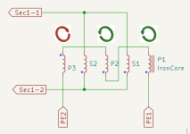
I don't think that is how I connected the windings, I'm 99% sure my diagram is correct, it can be confusing - the dot indicates the winding start and the arrow indicates the winding direction - I have left out the ultra linear taps as they only confuse the diagram further.

@50AE, did you mean this kind of winding arrangement?
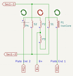
In conditions this is a SE transformer, PE1 represents the anode end, PE2 represents B+ end, and the outer B+ layer is reverse wound so that B+ end is closest to the secondary, then yes, this is correct and will give you a free lunch of P\S capacitance reduction.
OK, thanks. Applying same logic PP transformer B+ layer (usually in the mid) should be reverse wound? Outermost layers of primary must be 1/2 of inner ones, so I have drawn this explicitly.In conditions this is a SE transformer, PE1 represents the anode end, PE2 represents B+ end, and the outer B+ layer is reverse wound so that B+ end is closest to the secondary, then yes, this is correct and will give you a free lunch of P\S capacitance reduction.
Attachments
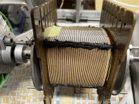
Here is a tip how to drastically reduce side effect of impregnation - increase of the parasitic capacitance. You fix winding turns with neutral silicone (like on picture attached), then not vacuum impregnate, but just immerse finished transformer into the can with varnish liquid for a short time. This is enough to fill the gaps and fix lamination sheets of the core. Silicone doesn't get absorbed into insulation material and therefore doesn't change its dielectric constant. Varnish need to be cured at 120C so neutral silicone is OK but other constructional adhesives like Soudal Fix All Crystal are not.
Attachments
You could that, yes, however in this case, by doing that within a mid package shifts this capacitance into the primary region. This is not necessarily a bad thing, where within most OPTs there is plenty of headroom to dump P\S capacitance into P-P capacitance. I find it useful to balance Cp and Cs, which can bring a very even frequency response despite variation of driving resistance. I usually aim, for 1:1 Cp to Cs ratio.OK, thanks. Applying same logic PP transformer B+ layer (usually in the mid) should be reverse wound? Outermost layers of primary must be 1/2 of inner ones, so I have drawn this explicitly.
As for the outer primary packages of the interleaving there will be increased voltage potential difference, where the capacitance path is bottom outer 1/2 primary -> core (floating) -> top outer 1/2 primary . But for most OPTs we can assume a thick bobbin with air in between and not a core touching full filling factor, so high distance and low epsilon take care of this.
If you're looking for low epsilon between windings, you could experiment with air dielectrics. One affordable way is to use polyester mesh for external display flags. It measured an epsilon between 1.2 and 1.3.
Probably my 40th or 50th sketch of designing a SE - PP 1 : 1+1 phase splitting transformer with the aim of delivering perfect amplitude balance between both halves over the whole frequency response range. All capacitances and leakage inductances have been balanced, including the primary shunt capacitance, where disbalance there will also affect the secondaries. This design is single-bobbin, although I also have double-bobbin designs, however with a different interleaving approach and different screening techniques.
Core grounding is also important, as floating core at specific potential will also affect secondary disbalance. In this case, there is double electrostatic screen. First screens are only floating and average the voltage gradient of the primary layer. Then secondary grounded screens balances the capacitances between the secondary packages, illustrated in green. The packages in brown-green are reverse-wound secondaries. The primaries are depicted in red and orange, where the red package is also reverse wound to shift capacitance towards the primary region. The secondaries are vertically split.
If this design turns out successful, I'll share it to the forum as contribution. For now it is just a teaser.
Last edited:
Always a pleasure to read from individuals with so much knowledge who also wish to share it. The truth is that I have never faced such a challenging task, neither with output transformers nor with phase-shifting interstages. I can't remember the number of transformers discarded because they didn't meet the design requirements.
We seek quality within certain parameters. This has no limits: the eternal battle between leakage inductance, capacitance, primary inductance, and efficiency. Achieving perfection in all these parameters is practically impossible unless weight or space are also infinite
When we perform calculations for leakage inductance and capacitance, and assess how these parameters impact the high-frequency band, we quickly see that capacitance is much more concerning. Typically, leakage inductance tends to roll off well above 150 kHz.
Apart from everything mentioned earlier, considerations such as adding gap between each layer and determining the minimum space between the primary and secondary windings are important. It's beneficial to wind the primary, especially in the upper layers, with a much larger surface area in the same direction. Take a look at the photo on this website; you can see how capacitance decreases significantly. This approach has yielded good results for me in transformers with heavy loads, such as those designed for the 211.
https://www.powersystemsdesign.com/articles/flyback-transformer-primary-winding-structures/18/5469
![1413383084_Fig%206[1].jpg](https://www.diyaudio.com/community/attachments/1413383084_fig-206-1-jpg.1244546/ "1413383084_Fig%206[1].jpg")
We seek quality within certain parameters. This has no limits: the eternal battle between leakage inductance, capacitance, primary inductance, and efficiency. Achieving perfection in all these parameters is practically impossible unless weight or space are also infinite
When we perform calculations for leakage inductance and capacitance, and assess how these parameters impact the high-frequency band, we quickly see that capacitance is much more concerning. Typically, leakage inductance tends to roll off well above 150 kHz.
Apart from everything mentioned earlier, considerations such as adding gap between each layer and determining the minimum space between the primary and secondary windings are important. It's beneficial to wind the primary, especially in the upper layers, with a much larger surface area in the same direction. Take a look at the photo on this website; you can see how capacitance decreases significantly. This approach has yielded good results for me in transformers with heavy loads, such as those designed for the 211.
https://www.powersystemsdesign.com/articles/flyback-transformer-primary-winding-structures/18/5469
Capacitance in audio transformers deserves a huge amount of discussion. There can be complex and unique combinations with leakage inductance that result into a win or loose situation.
Leakage inductance also requires more insight than most valuable books tell us. Different leakage inductances can coexist into a transformer. In the books, we're looking mostly at the primary to secondary Ls. For example, where a capacitance difference between two distant primary layers series couples them, a much higher Ls can manifest itself, more than the P/S calculated one. This alone can bring confusion among any attempts of calculating Ls/Cs/Cp by analyzing resonances.
What helps understanding output transformers is discretizing them into smaller transformers, where each layer with its unique Ls/Cp/Cs ratio is coupled to the rest. The more interleaves you add, the more the complex model becomes. A single change into the windings connection changes all Cp/Cs and additional Ls values.
As for vertical sectioning, in literally 98% cases of audio transformer design, I find little practical use. Yes, it does split self-primary capacitance of the layer, however:
1. In case it is sandwiched between two low-impedance secondary layers from both sides, you lose the benefit - from a square reduction of capacitance vs sections to 0.7 vs 1. (From small recollection, I believe 0.7 was the lower achievable capacitance reduction factor of a sandwiched vertically sectioned primary (Crowhurst))?
2. In most OPTs, self primary capacitance is already low, due to the high layer count (low voltage gradient) and high amount of series connections of the primary.
3. Your biggest offender is the P/S capacitance, especially at anode layers.
4. Vertical sectioning is valuable for air-core chokes. In ferromagnetic chokes, vertical sectioning "benefits" get shunted by the core. There is an optimum amount of vertical sectioning, where an extend beyond that increases capacitance instead of decreasing it. It is also depicted in transformer literature.
5. It is also valuable for kV applications, where you would require an ample amount of insulation between and low voltage gradient between layer ends.
Here's one of my modelling attempts on LTSpice. It depicts a transformer with a 1:1 ratio, S-P-S configuration, with 6 secondary and 6 primary layers. The purpose of the model is experimentation and observation, how different Ls, Cp and Cs values interact. The main drawback with modelling is, you have to be aware, theoretically of all Ls, Cp and Cs beforehand, of their values and placements, before sketching the model. Note that additional primary to primary leakage inductance resonant tanks are not added to this model.
Last edited:
This segmented winding (another variant is progressive layout) decreases only self-capacitance of the primary.Take a look at the photo on this website; you can see how capacitance decreases significantly.
In output transformers the most difficult parameter to decrease is primary to secondary capacitance.
As you can see :
The formula for the capacitance (CC) of a parallel plate capacitor is expressed as:
C=( ε⋅A) /d
Where:
Once you calculate the desired leakage inductance, only the distance 'd' remains.. always is a balance of everything, sure maybe there are more ways to optimize.
lundalh say that use only one primary pack per side in Core C ,
OPT or IT is infinite field of possibilities 🙂
The formula for the capacitance (CC) of a parallel plate capacitor is expressed as:
C=( ε⋅A) /d
Where:
- C is the capacitance in farads (F).
- ε is the permittivity of the material between the plates. It can be the permittivity of free space or vacuum (ε0ε0) or the permittivity of the material (ε=εr⋅ε0ε=εr⋅ε0), where εrεr is the relative permittivity or dielectric constant of the material.
- A is the area of one of the capacitor plates in square meters (m²).
- d is the separation distance between the plates in meters (m).
Once you calculate the desired leakage inductance, only the distance 'd' remains.. always is a balance of everything, sure maybe there are more ways to optimize.
lundalh say that use only one primary pack per side in Core C ,
OPT or IT is infinite field of possibilities 🙂
Yes, this is one part of solving the problem, calculating the static capacitance. However in transformer, you have effective capacitances, which are the result of static capacitance multiplied by capacitance factor.
Inside a typical OPT, where the secondary is considered grounded and at "zero" potential, the capacitance factor towards the secondary is highest at the anode and exponentially decreases while progressing to the B+ layers. It is safe to say, capacitance factor follows impedance.
For example, let's examine the following interleaving setting with 12 primary layers and 4 P/S interfaces.
(Secondary) // P12, P11, P10, P9, P8, P7 // (Secondary x2) // P6, P5, P4, P3, P2, P1 // (Secondary)
A simple and average way, also mentioned by Patrick Turner, is taking all primary layers closest to the secondaries, which are P12, P7, P6 and P1.
We are labeled from the highest potential (P12) if the anode is connected there, and (P1) at the B+ end (lowest voltage gradient)
Now we take the midpoint of each layer, for that we subtract 0.5 from each number.
That stands for P11,5, P6,5, P5,5, P0,5
Taking the midpoint is not the absolute accurate way, as capacitance changes exponentially with voltage gradient, but does the job well enough
To calculate the capacitance factor, we divide each primary number by the whole number of primary layers, and square it. So that becomes.
Cf1 = (11,5/12)^2 = 0,918
Cf2 = (6,5/12)^2 = 0,293
Cf3 = (5,5/12)^2 = 0,210
Cf4 = (0,5/12)^2 = 0,002
Cfsum = 1,423
Now, using your static capacitance for each P/S interface, you can multiply it by the equivalent capacitance factor. You can see it is the higher at the anode layer (Cf1) at 0,918, almost equal to the static capacitance. However at the B+ layer interface, Cf4 is almost zero. Knowing this, you can vary the thickness of your insulation. Make it thicker at the high capacitance points and thinner near B+ levels. By doing this, you can decrease the leakage inductance to some extent without too much increase of capacitance. Let's call it thickness varying insulation layering.
You can also move the anode layers far away from secondary layers. At the expense of redirecting (dump) that same capacitance somewhere else. For example, let's change the interleaving to.
P12, P11, P10 // Secondary // P7, P8, P9 ; P6 ; P5 ; P4 // Secondary // P1, P2, P3
In this scenario, the inner primary consisting of 6 layers is split into 3 x 2 packages. The first (P7, P8, P9 is reverse wound. The outer (P1, P2, P3) is also reverse wound. Some capacitance is dumped into the primary inner region with a Cf of ((P9-P6)/12)^2 = 0.063
Let's recalculate the capacitance factors, where the primary interfacing layers are now: P10, P7, P4, P1
Cf1 = (10,5/12)^2 = 0,765
Cf2 = (6,5/12)^2 = 0,293
Cf3 = (4,5/12)^2 = 0,140
Cf4 = (0,5/12)^2 = 0,002
Cfsum = 1,200
You can take the interleaving to a further step, however at the expense of winding complexity. Like this.
P6, P5, P4 // Secondary // P8, P10, P12, P11, P9, P7 // Secondary // P1, P2, P3.
In this scenario, you'll be winding the inner primary region into a snail-like progression, where the Anode layers start at the middle, then progress outwards, towards the secondary layers from both sides.
That will increase primary package capacitance by 4 times compared to normal winding. Considering however there is plenty of headroom into the primary region, one could safely do it for most cases.
Now, the capacitances become.
Cf1 = (7,5/12)^2 = 0,390
Cf2 = (6,5/12)^2 = 0,293
Cf3 = (3,5/12)^2 = 0,085
Cf4 = (0,5/12)^2 = 0,002
Cfsum = 0,77. This stands for 1,81 times decrease of P/S capacitance for the same amount of P/S interfaces, hence the same value of leakage inductance.
Last edited:
In this frequency response comparison, you can observe the power of capacitance dump. In this case, a S-P-S interleaving with ~70mH primary to secondary Ls. The first example features a Panode to PB+ standard winding progression. The second example has an internal Anode layer with a snailshell-like progression towards the secondary. The transformers were built for experimentation and demonstration purposes. We experience an increase of 4 times into the primary region, from 104pF to 416pF. However the P/S capacitance has decreased from 410pF to 2,52 pF. You can see that primary capacitance alone is much less harmful than P/S capacitance, especially in this case, where secondaries are connected in series.


- Home
- Amplifiers
- Tubes / Valves
- Show your transformer work (gallery)