I’d be looking at ICEO at the full 120 volts when screening old transistors. You want well under a milliamp. Those old Fairchild trannies are pretty good - back when them and Motorola were bitter rivals. Now it’s all the same.
Cooler running power resistors are always a good idea - especially on those old PCBs that blacken and turn brittle with heat (and time).
Cooler running power resistors are always a good idea - especially on those old PCBs that blacken and turn brittle with heat (and time).
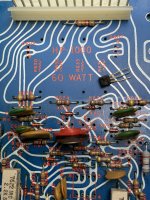
Removing components from the first driver board, I discovered 2 things:
1. A bad 2197 signal-level transistor
2. Underneath the now removed 5 watt emitter resistors, silk-screening that says HP-1000, or the lesser 60 watt brother. Maybe the HP-2000 uses it as well (hey, there is guy around here that remanufactured his HP-1000 driver boards)
Evidence attached.
1. A bad 2197 signal-level transistor
2. Underneath the now removed 5 watt emitter resistors, silk-screening that says HP-1000, or the lesser 60 watt brother. Maybe the HP-2000 uses it as well (hey, there is guy around here that remanufactured his HP-1000 driver boards)
Evidence attached.
Attachments
Finally, the parts arrived from Mouser yesterday.
I recapped the unit and got rid of a bunch of tantalum capacitors. The sound has cleaned up quite nicely.
Also, the new transistor recipe got installed on the board with great anticipation of yielding one good channel, but it would not be. I had to try three sets of outputs, one set was distorted, the other shorted out (good thing I was using a variac), the third seem to be almost OK but was unstable. Bias would not dial down below 150mV (1.8mV spec) and went to 600mV at the other end, even with new 1K ohm Bourns 25-turn potentiometers, and the outputs were warming up like in Class A. It also seemed to want to pop, run away and get loud. The sound was OK otherwise.
My conclusion is that either the circuit design is prone to instability, or more likely, my spare outputs are damaged or leaky and I need to throw them out.
One gain is that the LED Peak indicator was no longer triggered and the sound was not distorted with the third output set.
I reinstalled the class D output PCB and things are playing nice. I may leave it there as suggested, but after all the work on rebuilding the driver board, I may just try new output transistors, but not ready for a third Mouser expense just yet.
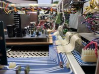
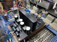
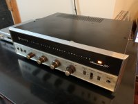
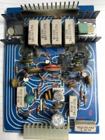
Some pictures will show the quality of the USA-made unit.
I recapped the unit and got rid of a bunch of tantalum capacitors. The sound has cleaned up quite nicely.
Also, the new transistor recipe got installed on the board with great anticipation of yielding one good channel, but it would not be. I had to try three sets of outputs, one set was distorted, the other shorted out (good thing I was using a variac), the third seem to be almost OK but was unstable. Bias would not dial down below 150mV (1.8mV spec) and went to 600mV at the other end, even with new 1K ohm Bourns 25-turn potentiometers, and the outputs were warming up like in Class A. It also seemed to want to pop, run away and get loud. The sound was OK otherwise.
My conclusion is that either the circuit design is prone to instability, or more likely, my spare outputs are damaged or leaky and I need to throw them out.
One gain is that the LED Peak indicator was no longer triggered and the sound was not distorted with the third output set.
I reinstalled the class D output PCB and things are playing nice. I may leave it there as suggested, but after all the work on rebuilding the driver board, I may just try new output transistors, but not ready for a third Mouser expense just yet.
Some pictures will show the quality of the USA-made unit.
Attachments
Last edited:
You didn't replace ALL the output transistors on a channel with new ones same part # from the same production datecode? Standard practice on meltdown amps. I've found overheated used transistors that test Iceo okay @ 2 v are not okay at rail voltage. Plus PNP & NPN should be same series, matching push pull if this amp is not quasi-comp. For example, 2n3055 from today is not even the same technology as a 1970 2n3055. Epitaxial versus homotaxial. If the amp is oscillating with epitaxials and was designed for homotaxials, you have to put a 10 ohm 2 watt resistor series the output transistor base. I put the resistor in place of the wire over to the heat sink from the driver.Finally, the parts arrived from Mouser yesterday.
the new transistor recipe got installed on the board with great anticipation of yielding one good channel, but it would not be. I had to try three sets of outputs, one set was distorted, the other shorted out (good thing I was using a variac), the third seem to be almost OK but was unstable. Bias would not dial down below 150mV (1.8mV spec) and went to 600mV at the other end, even with new 1K ohm Bourns 25-turn potentiometers, and the outputs were warming up like in Class A.
My conclusion is that either the circuit design is prone to instability, or more likely, my spare outputs are damaged or leaky and I need to throw them out.
You can detect ultrasonic osciallation without a scope. You use an analog voltmeter on 20 vac or 50 vac scale, with a .047 uf capacitor between the negative probe & the speaker ground. High steady voltage, likely an oscillation. You can prove it by changing .047 cap to 390 pf. 390 pf will block music, but pass ultrasonic right through to the meter. I use a 200 v rated cap. You can salvage one from a switcher power supply if you don't want to buy one. The alligator clip leads you have to buy. The $7 package of 10 clip leads from parts-express is a lot cheaper than the $70 package of 10 clip leads from pamona via newark mouser or digikey.
If idle bias is still above 25 ma, short a spreader diode or two. The diodes between the bases of the two driver transistors. If that drives bias too low, you can replace the short with a resistor of a value suitable to put the pot into the middle of its range at 25 ma. You don't have to butcher the board, you can tack parallel wire or resistor on top of the existing spreader diodes.
Last edited:
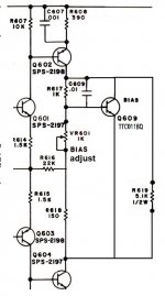
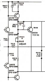
This one uses a vbe multiplier, and with the resistor values should be able to bias the outputs completely OFF. That does suggest it could be oscillating if it won’t bias all the way down. Could try temporarily shorting the vbe multiplier to rule out other possible mishaps. The vbe transistor could be open and not working at all. Then the bias would be too high regardless of setting.
The original outputs were epitaxial. 2N5630/6030 did not have a hometaxial equivalent. The drivers might have been run of the mill TIP-like epitaxials, but my gut tells me they were faster. Maybe not MJE15030-fast, but faster than 2N5630’s. If it is oscillating, base stoppers on the drivers may be necessary - but it is unusual for EF2’s to oscillate by themselves. The circuit might have been counting on a high-ish collector base capacitance in the driver for lag compensation of the VAS - but that’s not really the driver transistor‘s fault - just careless design.
The original outputs were epitaxial. 2N5630/6030 did not have a hometaxial equivalent. The drivers might have been run of the mill TIP-like epitaxials, but my gut tells me they were faster. Maybe not MJE15030-fast, but faster than 2N5630’s. If it is oscillating, base stoppers on the drivers may be necessary - but it is unusual for EF2’s to oscillate by themselves. The circuit might have been counting on a high-ish collector base capacitance in the driver for lag compensation of the VAS - but that’s not really the driver transistor‘s fault - just careless design.
Thanks for your thoughtful replies and I will digest them carefully, it does confirm my lack of confidence in the circuit design. And yes indianajo, I normally always do the full chain in new transistors, taking a shortcut with used outputs did not save anything. I will need to purchase four outputs to prove success. They are more than twice what I am used to paying for them now.
This exercise reminds me of a couple challenging Sansui 9090DBs where I had to replace every transistor from input pair to outputs. The circuit however was rather stable in comparison, and it was a good outcome. Lots of late nights comparing datasheets.
My understanding, however, is not on par with your replies, but I will put my head into them.
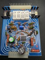
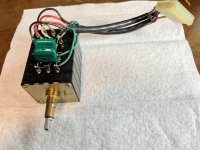
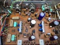
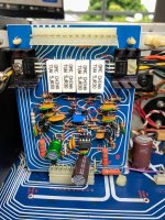
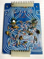
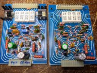
Not to change the subject too much, here is a re-transistorizing that I did without any soldering, all transistors new and socketed.
This exercise reminds me of a couple challenging Sansui 9090DBs where I had to replace every transistor from input pair to outputs. The circuit however was rather stable in comparison, and it was a good outcome. Lots of late nights comparing datasheets.
My understanding, however, is not on par with your replies, but I will put my head into them.
Not to change the subject too much, here is a re-transistorizing that I did without any soldering, all transistors new and socketed.
Attachments
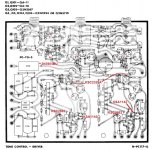
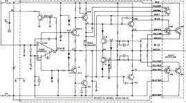
I extracted the vbe multiplier circuit (from the schematic), it is attached. If I do get this thing working, I will need to see it in action on a scope and see if there is crossover distortion. R619 is just a bit downstream, but it is represented. The vbe transistor is new.This one uses a vbe multiplier, and with the resistor values should be able to bias the outputs completely OFF. That does suggest it could be oscillating if it won’t bias all the way down. Could try temporarily shorting the vbe multiplier to rule out other possible mishaps. The vbe transistor could be open and not working at all. Then the bias would be too high regardless of setting.
Attachments

Sorry to keep you all in suspense.
I broke the piggy bank yesterday and ordered the 8 output transistors from Digikey. I decided on the MJ15003G and MJ15004G. $80 for all 8 shipped.
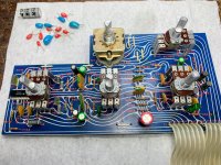
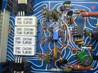
The rebuilt driver board sure looks lonely waiting for these outputs to arrive.
If things still sound distorted or I can't achieve bias voltage specification, I am going to need some armchair advice. The preamplifier sounds quite stellar.
I broke the piggy bank yesterday and ordered the 8 output transistors from Digikey. I decided on the MJ15003G and MJ15004G. $80 for all 8 shipped.
The rebuilt driver board sure looks lonely waiting for these outputs to arrive.
If things still sound distorted or I can't achieve bias voltage specification, I am going to need some armchair advice. The preamplifier sounds quite stellar.
Attachments

The new output transistors arrived today, so the saga continues.This one uses a vbe multiplier, and with the resistor values should be able to bias the outputs completely OFF. That does suggest it could be oscillating if it won’t bias all the way down. Could try temporarily shorting the vbe multiplier to rule out other possible mishaps. The vbe transistor could be open and not working at all. Then the bias would be too high regardless of setting.
The original outputs were epitaxial. 2N5630/6030 did not have a hometaxial equivalent. The drivers might have been run of the mill TIP-like epitaxials, but my gut tells me they were faster. Maybe not MJE15030-fast, but faster than 2N5630’s. If it is oscillating, base stoppers on the drivers may be necessary - but it is unusual for EF2’s to oscillate by themselves. The circuit might have been counting on a high-ish collector base capacitance in the driver for lag compensation of the VAS - but that’s not really the driver transistor‘s fault - just careless design.
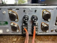
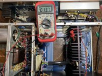
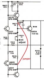
The unit was in protection when I tried the new output transistors--the variac bulb was full bright. The problem is confirmed to be in the driver board. The new driver transistors--with outputs disconnected--I think were oscillating as they were measuring 3.5 VDC instead of the spec .5 VDC at the emitters, heat sinks quite warm. I had to short out the vbe multiplier (as shown with the white wire jumper) before it would get the drivers down to the .5 VDC spec and run cool.
I reconnected the outputs, and it did come out of protection, but the sound is way distorted (sample). Maybe the op amp is damaged or ???
If you all have an idea how to reengineer the vbe multiplier circuit, removing the jumper, and perhaps adjusting the resistors, I am all ears.
Bias is up past 15 mV with a spec of 1.8 mV.
I ran out of time to find a single op amp 8-DIP, I think I have some in a DAC. Will pick up tomorrow with another single op amp and see if sound is ok, it is the only semi conductor--beside the diodes--that is not new in the chain.
The design yields no confidence, let's see if we can improve it with your help.
Thanks.
Attachments
To check, hack a source like a radio with volume control to use as a pre-amp.
Feed that signal to the main amp section.
That will allow you to decide if the op amp is defective.
Feed that signal to the main amp section.
That will allow you to decide if the op amp is defective.
A good NE5534 single op amp went in, and the music is crystal clear. So all along, I have been using a damaged op amp. I need to just throw a bunch of semis out.
BIAS voltage is not bad at 1.3 mV (spec 1.8 mV). I may leave the bias pot and resistors bypassed, unless you all have suggestions. It is fixed at the 1.3 mV.
BIAS voltage is not bad at 1.3 mV (spec 1.8 mV). I may leave the bias pot and resistors bypassed, unless you all have suggestions. It is fixed at the 1.3 mV.
Attachments
If the bias stack is strapped you should get zero bias in the output stage. Are you measuring the voltage on the emitter resistor with no load? If you do have the speaker connected any current due to the output offset voltage will upset the reading.
And are you absolutely positive the Toshiba transistor you used is hooked up correctly? With the writing on the TOP it goes ECB, backwards from a TO-220. Otherwise, there is no way NOT to be able to adjust it down unless the pot is flaky.
The op amps can and do get damaged in these circuits when you short the output transistors and throw the full rail voltage at the speaker. What happens is that the full rail voltage gets applied to the feedback as well, and if the current limiting is insufficient the inputs (or perhaps output) of the op amp can get blown. 5532/4 happens to be one of the more rugged ones. Some of the really nice ones will die if you drive the inputs so much as a few tens of micro amps above the rail and are not suitable for service here. Even the old 351 will take around 10 mA into the input stage before crying uncle.
Last edited:
You are right on! Took speaker cable off, bias reading went to "0"If the bias stack is strapped you should get zero bias in the output stage. Are you measuring the voltage on the emitter resistor with no load? If you do have the speaker connected any current due to the output offset voltage will upset the reading.
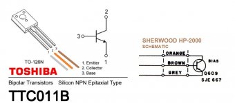
I checked the pinout of the Toshiba and it is identical to the SJE667, I attach a piece of the Toshiba datasheet.And are you absolutely positive the Toshiba transistor you used is hooked up correctly? With the writing on the TOP it goes ECB, backwards from a TO-220. Otherwise, there is no way NOT to be able to adjust it down unless the pot is flaky.
I will order some NE5534 then, these I am borrowing from a DAC. In the past, I've had some fail from just static shock to a chassis, several actually of the hi-fi variant.The op amps can and do get damaged in these circuits when you short the output transistors and throw the full rail voltage at the speaker. What happens is that the full rail voltage gets applied to the feedback as well, and if the current limiting is insufficient the inputs (or perhaps output) of the op amp can get blown. 5532/4 happens to be one of the more rugged ones. Some of the really nice ones will die if you drive the inputs so much as a few tens of micro amps above the rail and are not suitable for service here. Even the old 351 will take around 10 mA into the input stage before crying uncle.
Next step: If I remove the jumper from the bias stack, I am back at an unstable situation. Should I bypass R617 and R618 and see where that lands me? The pot is good, I checked before installation.
Attachments
I tried several resistors in R617 until I found that a 562 ohm resistor gave enough room with the trimpot to dial bias easily at 1.8 mV as specified by the SM. So R627 went from 1K to 562 ohms. The variable trimpot is at about 65 ohms. The circuit does slowly drift a bit, but I will take what I can get for now. The unit draws about 28-30 watts from the wall, as also specified by the SM, but this is with only one output channel connected. Sounds nice.
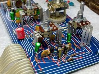
Now we move on to reviving the other side fire-starter driver board. Notice the condition of the bias resistors R617 and R618. Scary!
Now we move on to reviving the other side fire-starter driver board. Notice the condition of the bias resistors R617 and R618. Scary!
Attachments
Last edited:
Something here does not add up. You SHOULD be able to set the pot to 232 ohms (or somewhere close) with the original 1k and get the very same result. It is about the right number of Vbe’s so the pot setting makes sense. Does that 1k resistor actually measure 1k or did it get damaged and go high?
That's what I thought! But after a while I just went monkey replacing resistors until one finally worked. I should be able to have some time for measuring the trimpot this week. I think it is fine since these are mostly new parts and have not taken a beating yet without the safety of the variac.Something here does not add up. You SHOULD be able to set the pot to 232 ohms (or somewhere close) with the original 1k and get the very same result. It is about the right number of Vbe’s so the pot setting makes sense. Does that 1k resistor actually measure 1k or did it get damaged and go high?

Actually I was talking about the 1k fixed resistor that you replaced with a 560 ohm. If that had gone way high (say up in the 3 to 5 k range) you’d have trouble getting the bias down where it’s supposed to be. With it at 560 ohms, youre already running the trim pot down very close to its minimum just to get the bias up where it’s supposed to be. There wouldn’t be that much of a jump between 1k and 560 in that base-collector position where you would expect the pot to run out of adjustment range. IIRC, you had to replace the transistor and the pot - other resistors in the area could have been ****** too.That's what I thought! But after a while I just went monkey replacing resistors until one finally worked. I should be able to have some time for measuring the trimpot this week. I think it is fine since these are mostly new parts and have not taken a beating yet without the safety of the variac.
- Home
- Amplifiers
- Solid State
- Sherwood HP-2000, Resurrection, should I even bother...