I dived deep into this subject like many others. It would be great if we could use this thread to just share our projects and our experiences. Might they be technical (implementations) or listening reviews (subjective no problem it is just about sharing your experience)
I would like to avoid discussions if this all make sense, again, just sharing your work and experience.
Reason is, we might pick up ideas on implementation or also find inspiration to try out other clocks in our DAC systems.
having said so, also non DAC applications would be welcomed here (like ethernet switches for example or ADC ?)
Looking forward to your inputs and many pictures. I will take the lead with Post #2 🙂
.
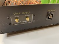
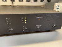
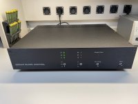
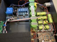
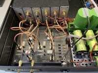
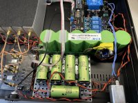
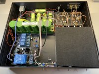
Yesterday evening I closed the chassis for the clock project - meaning everything works fine now. I tested everything with my bench DAC which is a RPI with the FiFoPi from Ian Canada. The clock is going to the sinePI squarer from Ian.
There was one problem though with the automatic switching. For that I need the L/R clock signal to determine the FS rate. I thought I could pick this from the NON-Isolated side on the FIFOPI - well.... wrong .... The problem was solved though by picking the L/R signal directly from the GPIO at the RPI....
Today I will get the clock signals and FS signal connected to my Audio Rack DAC and will be able to do (finally) the listening review on the doublers when yes or no in series with the basic clock.
below are some pictures of the current state of work
Attachments
-
 2021-11-09_20-27-51_IMG_6229.JPG411.5 KB · Views: 220
 -
 2021-11-09_20-32-32_IMG_6237.JPG386.8 KB · Views: 216
 -
 2021-11-09_20-33-20_IMG_6239.JPG382.8 KB · Views: 204
 -
 2021-11-09_20-27-06_IMG_6226.JPG788.5 KB · Views: 201
 -
 2021-11-09_20-27-24_IMG_6227.JPG788.2 KB · Views: 208
 -
 2021-11-09_20-27-30_IMG_6228.JPG796.9 KB · Views: 172
 -
 2021-11-09_20-26-51_IMG_6224.JPG792.6 KB · Views: 151
 -
 2021-11-09_20-26-59_IMG_6225.JPG731.9 KB · Views: 161
I just posted the final clock blog.
it covers the Andrea Mori clocks with and without doublers and the Ian Canada SinePi and ReclockPi as well
have a nice read 🙂
Doede
Link to Post of the final clock reviews

it covers the Andrea Mori clocks with and without doublers and the Ian Canada SinePi and ReclockPi as well
have a nice read 🙂
Doede
Link to Post of the final clock reviews
Doede,
IIUC noticed one thing in your blog writeup I would suggest to doublecheck on. That is the way BCLK is processed in FIFO_Pi. In the version of FIFO_Pi I have here, all the I2S signals are reclocked by MCLK on FIFI_Pi using a multi-channel D-Flip Flop IC just before they are sent out to the RPi GPIO bus. In other words, the signals don't come directly from the ASIC without isolation and reclocking.
Seems to me the purpose of Reclock_Pi is to do I2S reclocking one final time in a more optimal way than can be done on FIFO_Pi. Less noise to pick up on a separate PCB with its own ground plane and power rails, and less ground bounce on I2S signals since Reclock_Pi has all four signals on separate D-Flip Flop chips.
Excellent point Mark, you are right I did not really expressed it well and will change it ! Thanks for the notice
Not sure why this was moved to the vendor bazar. To make clear, I am not selling any clocks, just reviewing and showing my personal build . But never mind…